Content last revised on October 21, 2026
Field Diagnostics & Commissioning: DC-Link Capacitance Bank Layout and Low-ES in FF1200R17IP5 Topologies
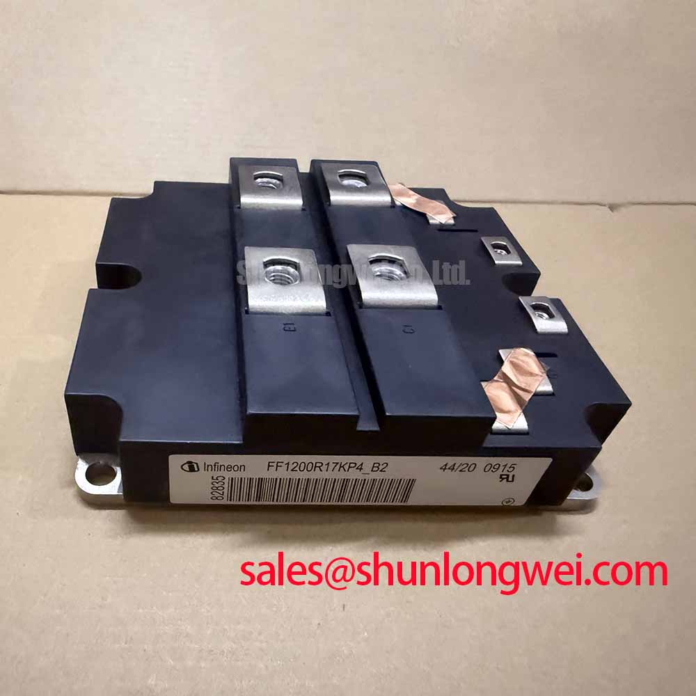
I check the discharged DC-link connections and capacitor-bank return path before investigating a turn-off voltage spike at the FF1200R17IP5. As a Design Consideration, the inspection should follow the actual commutation loop through the local capacitors, module terminals, and return conductors rather than judging the layout by cabinet appearance. Loose joints, displaced busbar connections, or a replacement capacitor with different connection geometry can change the transient response without changing the nominal DC voltage.
The supplied official specifications establish the module’s electrical and thermal reference points. The typical saturation voltage is an operating-point-dependent characteristic, not a fixed voltage drop across every load condition.
| Official Specification | Value | Engineering interpretation |
|---|---|---|
| Collector-emitter blocking voltage, VCES | 1700 V | Device blocking limit, not a prescribed DC-link operating voltage |
| Nominal collector current, IC(nom) | 1200 A | Nominal current rating subject to datasheet operating conditions |
| Maximum specified junction temperature | 150 °C | Junction limit, not an enclosure or heatsink temperature rating |
| Typical collector-emitter saturation voltage | 2.10 V | Consult Datasheet for measurement conditions |
| IGBT junction-to-case thermal resistance | 27 mK/W | IGBT thermal path; excludes the external cooling assembly |
| Diode junction-to-case thermal resistance | 47 mK/W | Diode thermal path; evaluate with diode losses |
| Package | P5 | Mechanical compatibility requires the module drawing |
As an Engineering Calculation, the first-order relationship Vpeak = VDC + Lσ × (di/dt) explains why stray inductance raises the turn-off voltage above the DC-link level. It is an estimate rather than a complete ringing model. A compact, overlapping outgoing and return busbar arrangement can reduce loop inductance, but acceptance should depend on measured collector-emitter peaks across the intended operating envelope, not an arbitrary universal inductance target.
Design Consideration: select local snubber capacitance from the measured transient energy, permissible voltage excursion, capacitor pulse capability, and resulting losses. A coordinated MOV network requires separate checks of repetitive operating voltage, clamping behavior, absorbed energy, temperature dependence, and protective disconnection. An upstream MOV should not be assumed to intercept a fast transient generated inside the local switching loop. Preserve insulation spacing when moving either component closer to the module.
For replacement assessment, compare the FF1200R17IP5 with candidates such as FZ1200R17KF6-B2 by circuit configuration, terminal arrangement, mounting drawing, switching behavior, and driver requirements. A related part designation does not establish interchangeability.
Transient Dynamics & Electrical Design: Diode Softness Factor Optimization via Sy on FF1200R17IP5
Capture diode recovery current together with collector-emitter voltage when investigating commutation ringing. Design Consideration: compare waveforms at matched load current, junction-temperature conditions, DC-link voltage, and gate-drive settings. Reverse-recovery peak current and the abruptness of its decay influence the transient, but probe placement and measurement bandwidth can also change the apparent waveform. A softness factor or “Sy” value is meaningful only when its definition and measurement conditions are established.
As an Engineering Recommendation, evaluate turn-on gate resistance and an RC snubber as interacting adjustments rather than independent cures. Slower current transfer can reduce recovery stress while increasing switching loss; damping can suppress oscillation while adding resistor and capacitor heating. Record both the electrical waveform and the temperature response before accepting a change. Compare with the original drive configuration instead of applying an unsupported resistance or capacitance value.
High-side gate-power integrity deserves its own measurement. If the system uses a bootstrap supply, its capacitor must support gate-charge demand, driver quiescent consumption, leakage, and the longest interval between recharge opportunities while retaining the driver’s required supply margin. Duty cycle, startup behavior, and recharge-path losses determine suitability. Where an isolated supply is used, investigate its transient regulation and local decoupling rather than applying bootstrap sizing rules.
Design Consideration: when reviewing other switching positions in the same converter, assess devices such as FZ2400R17HP4_B29 against their own circuit role and driver requirements; this reference does not identify that device as a front-end rectifier or a substitute. Potential FF1200R17IP5 applications include multi-megawatt wind-turbine full-scale converters and bidirectional battery DC-DC stages, subject to topology, cooling, protection, and mechanical compatibility assessment.
FF1200R17IP5 Operational Boundaries: Evaluating Active Miller Clamp Implementation Limits
Measure the inactive switch’s gate-to-emitter waveform during opposite-switch commutation before attributing an overcurrent trip to false turn-on. Design Consideration: collector-voltage transitions can couple current into the gate circuit, while common return impedance can distort the effective gate voltage. Observe the signal at the module’s designated gate and emitter connections with a suitable measurement arrangement; a remote driver-board measurement can conceal local excursions.
An active Miller clamp provides a low-impedance discharge path only within its specified activation conditions and current capability. As an Engineering Recommendation, review clamp engagement timing, the physical discharge loop, driver sink capability, and behavior during undervoltage or loss of control power. Negative gate bias is a system-level option whose magnitude must remain within the module and driver limits throughout switching and fault transients; it is not a universal prescription for this model.
Design Consideration: compare the optocoupler or digital isolator’s specified common-mode transient immunity with the measured isolation-barrier disturbance. Simultaneously observing driver input, output, and supply behavior helps distinguish isolation-path disturbance from gate-loop coupling. Changing gate damping alone may leave a command-path problem unresolved. For device-family context, the Infineon IGBT Modules & Discretes Official Portfolio provides the manufacturer’s starting point for product and documentation selection.
Clearance and creepage around module terminals and driver connections require separate assessment under the equipment’s applicable insulation-coordination requirements. Working voltage, impulse exposure, pollution conditions, insulating materials, and installation altitude influence that assessment. During maintenance, remove conductive contamination using approved methods and inspect barriers for damage; cleaning does not correct insufficient geometric spacing.
Maintenance Note: Trend terminal temperature rise and heatsink airflow during scheduled inspections, and verify connection tightening only with the equipment isolated and the specified procedure available.
Preventing Spurious Faults: Cosmic Ray Robustness and Voltage Derating Guidelines for FF1200R17IP5
Separate recoverable protection trips from destructive device failures before assigning a cosmic-ray explanation. As a Design Consideration, retain the event log, DC-bus history, switching traces, temperature records, installation elevation, and protection response. These observations support investigation without treating an unexplained event as proof of single-event burnout.
For a cosmic-ray robustness assessment, request manufacturer-supported reliability information covering the relevant blocking voltage, temperature, and installation environment. Any FIT estimate or voltage-derating curve needs an identified source, applicable test basis, and operating assumptions. The 1700 V blocking specification alone supplies neither a cosmic-ray failure rate nor an altitude-dependent operating limit. A “Cu” guideline should not be treated as a manufacturer-defined coefficient without its documented definition.
Engineering Recommendation: keep environmental inspection actionable while that assessment proceeds. Set heatsink cleaning and thermal-interface inspection intervals from contamination trends, operating hours, temperature history, and equipment instructions rather than an invented module service interval. Examine thermal-interface condition during authorized disassembly and maintain consistent mounting practice. For reversible power flow, review temperature excursions during charging, discharging, and standby transitions instead of interpreting a steady heatsink reading as evidence of low thermal cycling.
Design Consideration: prevent condensation through enclosure management appropriate to the installation, and inspect moisture-affected terminal areas before re-energization. Broader technology comparisons in Wide Bandgap Revolution provide background on GaN and SiC integration tradeoffs, not FF1200R17IP5 lifetime evidence. Close the maintenance work order with recorded temperatures, connection checks, environmental observations, and protection-test results so subsequent inspections can identify change against an established baseline.