Content last revised on October 19, 2026
Transient Dynamics & Electrical Design: Fault Clearing Dynamics of FS225R12OE4
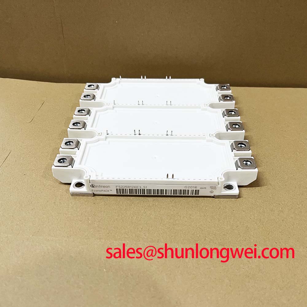
When a traction inverter trips during regenerative braking, I first isolate the gate driver supply and inspect the switching waveform at the module terminals before applying another high energy test. The FS225R12OE4 is specified with a 1200 V collector emitter voltage, a 225 A continuous DC collector current at TH = 80°C, and an integrated free wheeling diode rated for a 450 A repetitive peak forward current at tp = 1 ms. These are the hardware boundaries used when evaluating a low voltage traction inverter, brake chopper, or bidirectional battery converter.
Short circuit protection must be treated as a coordinated gate driver function rather than an assumed property of the module. A type I desaturation response detects a rapid loss of collector emitter saturation after the driver has commanded conduction. A type II response is useful when the first response is influenced by blanking time, switching noise, or a high current commutation event. For this application, the protection chain should be capable of identifying the fault within the specified sub 10 µs protection objective used by the system design, then reducing gate current in controlled stages. The module rating itself does not establish a universal short circuit withstand time, so the protection timing, gate resistance, current path inductance, and test conditions must be validated together.
Two stage soft turn off is preferable to an abrupt gate discharge when the fault current is already high. The first stage limits the rate of current interruption and helps control the inductive voltage rise. The second stage brings the gate to its defined off state after the primary overshoot has settled. During commissioning, place the current probe and differential voltage probe so that the measured loop includes the actual power terminals and commutation path. A waveform that looks acceptable at the driver board can still conceal excessive voltage at the module because of stray inductance between the board and the power bus.
For regenerative braking, the braking resistor and chopper transistor must absorb the recovered electrical energy without allowing the DC link to approach the module voltage boundary. The energy management controller determines the braking duty cycle, resistor temperature limit, and fault response. The FS225R12OE4 contributes the switching path; it does not independently define the permissible DC link operating point. Designers should verify the collector emitter peak voltage during turn off, diode recovery, braking transitions, and battery contactor events.
A bootstrap powered high side driver also deserves attention during repeated traction reversals. The bootstrap capacitor is charged and discharged by the actual switching pattern, gate charge, driver consumption, leakage, and diode recovery behavior. Check that the capacitor voltage remains inside the gate driver operating window during the longest high side interval and the most demanding repetitive charge cycle. Do not infer this margin from the module current rating. The selected bootstrap diode, capacitor, and charging path should be evaluated at the switching frequency and temperature used by the complete inverter.
For an independent device reference, engineers can review the Infineon IGBT Modules & Discretes Official Portfolio and the Infineon IGBT Discretes & Co-Pack Diodes. These resources help separate module level ratings from the system level requirements imposed by a traction inverter.
| Parameter | Official value | Engineering significance |
|---|---|---|
| Collector emitter voltage | VCES: 1200 V | Voltage boundary for the switching device |
| Continuous DC collector current | IC nom: 225 A at TH = 80°C | Current rating under the stated case temperature condition |
| Collector emitter saturation voltage | VCE sat: 1.85 V typical at Tvj = 25°C and VGE = 15 V | Conduction loss reference under the stated test condition |
| Junction to heatsink thermal resistance | RthJH: 0.160 K/W per IGBT | Thermal path reference for heatsink evaluation |
| Operating junction temperature | Tvj op: −40°C to 150°C | Specified junction temperature operating range |
Preventing Spurious Faults: Main Terminal Pinout Mechanical Alignment Guidelines for FS225R12OE4
Mechanical alignment at the main terminals should be checked before diagnosing a repeated overcurrent or desaturation alarm. A power cable that is pulled sideways by a rigid busbar can transfer levering force into the module terminal assembly. That stress may become more severe as the assembly cycles between cold start and high junction temperature. Align the busbar naturally with the terminal faces, confirm that the washers seat evenly, and ensure that the screw thread engagement matches the approved hardware arrangement for the module and busbar.
Use a torque controlled tool and follow the manufacturer’s mechanical installation data for the actual terminal and fastener configuration. Do not use tightening force to correct a misaligned copper bar. The correct sequence is to remove the mechanical side load, seat the conductor flat, and then tighten the approved hardware in the specified order. After thermal cycling, inspect for movement, discoloration, lifted washers, or a change in terminal seating. These checks are more useful than repeatedly replacing a module while the busbar remains under mechanical tension.
⚠️ Field Alert: Never apply a guessed tightening torque or force a rigid busbar into alignment, because the resulting stress can damage the terminal assembly or distort the thermal interface.
Parallel module operation requires a symmetrical power path. Differences in busbar length, joint resistance, and cooling conditions can cause one module to carry more current than another. The positive temperature coefficient associated with the stated VCE sat operating behavior can support static current sharing, but it does not correct an asymmetrical layout or a poorly seated terminal. Match the collector and emitter path geometry, keep the gate drive references consistent, and measure each branch under the same operating condition.
When checking a suspected current imbalance, compare the voltage drop across each conduction path and inspect the switching node with a properly rated differential probe. A thermal image can identify an uneven branch, but it should be interpreted alongside gate timing, busbar geometry, and heatsink contact. The FS225R12OE4 has a stated typical saturation voltage of 1.85 V at Tvj = 25°C and VGE = 15 V; that value is a test condition, not a universal field threshold for every temperature, current, and gate drive state.
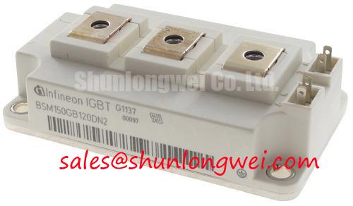
In a forklift traction system, the same mechanical discipline applies to the brake chopper, inverter leg, and bidirectional DC to DC stage. Battery charging and regenerative discharge create repeated thermal transitions, so cable routing should avoid transmitting vibration into the module terminals. The related BSM35GD120DN2E3224 may be evaluated as a separate replacement option only after its voltage, current, package, terminal arrangement, gate requirements, and thermal interface have been matched against the original system design.
Assembly Integrity & Layout Architecture: PCB Symmetry Considerations for Dual IGBT
The gate return path must be separated from the high current emitter path wherever the module and driver provide the corresponding auxiliary connection. A shared copper section allows emitter current transients to modulate the driver reference, creating apparent gate voltage movement and possible oscillation. Route the driver return directly to its intended emitter reference, while the main power return follows the low impedance switching path. The two paths should meet only where the module and gate driver architecture require them to meet.
Keep the turn on and turn off gate loops compact, with the gate resistor and any damping components placed according to the driver layout objective. Minimize the area exposed to the collector switching node, maintain appropriate clearance around high dv/dt conductors, and avoid running control traces in parallel with the main commutation path. The final spacing is determined by the insulation system, working voltage, pollution environment, board material, and applicable equipment standard, not by the IGBT current rating alone.
During a fault investigation, monitor the gate to emitter voltage directly at the module rather than at the controller connector. Compare the waveform during normal traction, regenerative braking, and a controlled low energy test. A negative gate excursion, unexpected plateau, or ringing pattern may indicate mutual coupling or an unsuitable return path. Correct the physical routing first, then retune the gate network using the measured switching behavior. A driver board that passes a bench test can behave differently after the long power bus, heatsink, and battery cable are installed.
The thermal interface is equally important to assembly integrity. The specified RthJH of 0.160 K/W per IGBT assumes the intended junction to heatsink path and should be considered together with the heatsink resistance, interface material, mounting flatness, and clamping method. Apply the approved thermal interface material as a uniform thin layer without trapped air or contamination, and use the module manufacturer’s installation sequence for screw tightening. Excess compound can increase interface variation, while insufficient coverage can leave local dry areas.
For a dual IGBT layout, place the power loop, gate loop, and auxiliary emitter reference so that one switching device does not inject its transient current into the other device’s control return. Symmetrical copper geometry is helpful when the two devices share current, but symmetry must include the driver paths, terminal connections, cooling contact, and measurement points. When the module is used in a bidirectional battery converter, evaluate both charge and discharge directions because the active switching device and free wheeling path change with power flow.
The front end may include a rectifier or auxiliary conversion stage such as BSM300GA120DN2FS. Its presence does not establish compatibility with the FS225R12OE4; the complete DC link, gate drive, protection timing, thermal path, and terminal topology still require system verification. For gate drive investigations involving off bias and transient immunity, the reference article Evolution of Negative Off-Bias Gate Drive Circuits provides useful background for selecting and testing the control strategy.
Before returning a forklift or warehouse traction controller to service, record the cold terminal condition, confirm the busbar alignment, inspect the thermal interface, and compare the gate and collector emitter waveforms under a controlled load. The module’s official operating junction range of −40°C to 150°C supports the temperature boundary for evaluation, while the inverter controller, cooling system, battery profile, and enclosure determine whether the installed assembly remains within that boundary during repeated duty cycles.