

Content last revised on September 27, 2026
Preventing Spurious Faults: Optocoupler vs Digital Coreless Transformer Guidelines for FS820R08A6P2LB
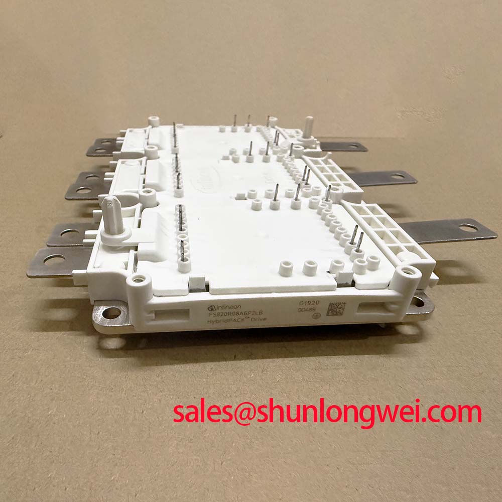
Verify the equipment’s DC link voltage, module marking, and power terminal connections before fitting an FS820R08A6P2LB, then compare the gate driver and cooling assembly with the original equipment documentation. The decisive electrical boundary is its 750 V collector-emitter rating: this is a device limit, not permission to connect the module directly across a higher-voltage DC bus. An apparently matching footprint does not establish electrical compatibility, protection coordination, or thermal suitability.
The Infineon FS820R08A6P2LB IGBT module has the following official specification values. Current capability must be interpreted alongside the manufacturer’s operating conditions, cooling requirements, and safe operating area; the nominal current is not an unconditional continuous output rating for the completed inverter.
| Parameter | Official Specification | Integration significance |
|---|---|---|
| Collector-emitter voltage | 750 V | Check maximum blocking stress, including switching overshoot. |
| Nominal collector current | 820 A | Evaluate against the specified thermal and electrical test conditions. |
| Operating junction temperature | −40°C to 150°C | Use the operating range when assessing junction temperature throughout the load cycle. |
| Maximum specified junction temperature | 175°C | Do not treat this limit as a continuous operating target. |
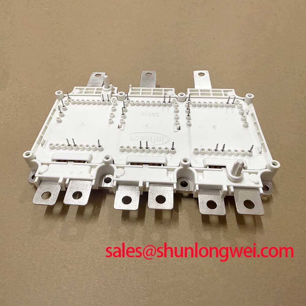
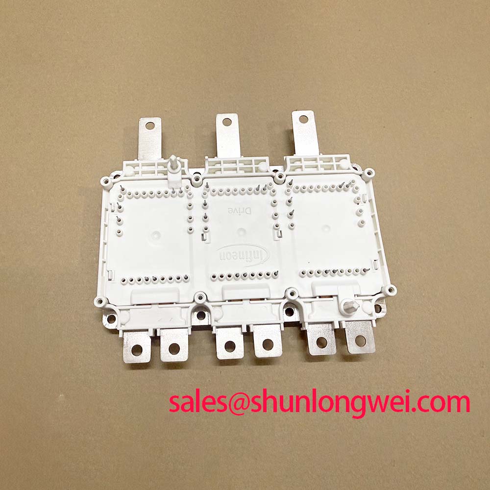
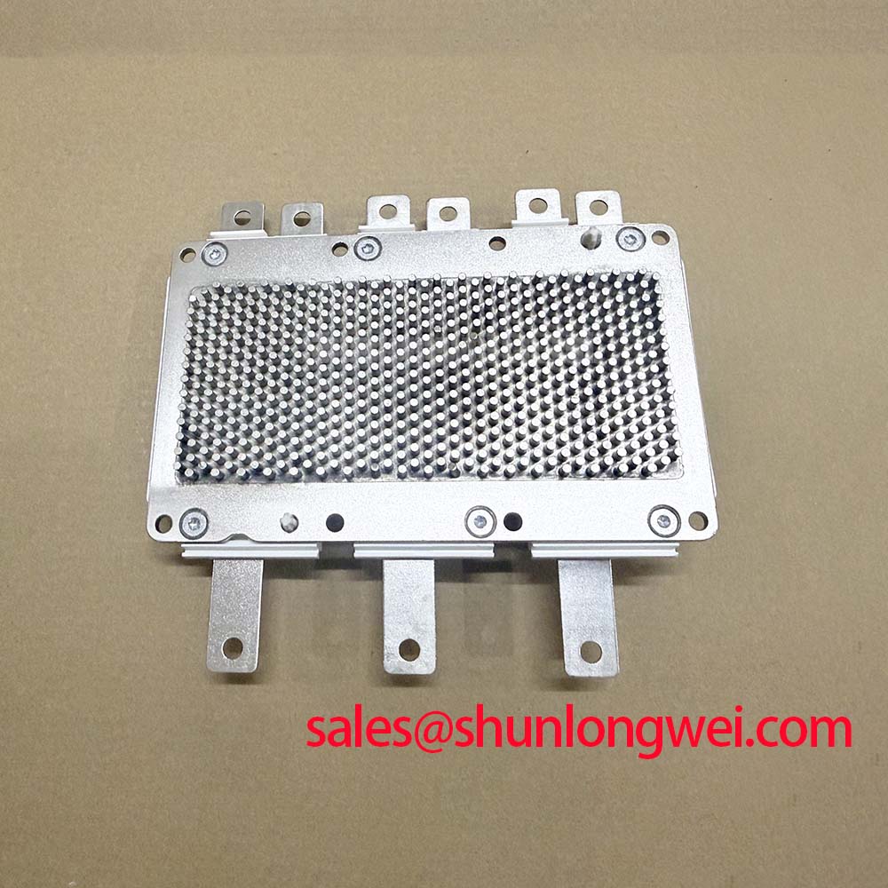
| Package | HybridPACK™ Drive | Confirm the exact mechanical drawing, cooling interface, and terminal arrangement. |
| Technology designation | Infineon EDT2 | Use model-specific switching and thermal characteristics for qualification. |
Preventing Spurious Faults: Optocoupler vs Digital Coreless Transformer Guidelines for FS820R08A6P2LB
Start a false-trigger investigation at the module’s gate-emitter connection rather than at the controller output alone. As a Design Consideration, compare the commanded switching state with the actual gate voltage, driver supply voltage, and fault signal during the same switching event. Use appropriately rated differential measurement equipment and short probe connections. Probe pickup can resemble gate ringing, so repeat questionable measurements with a controlled measurement arrangement before changing the driver circuit.
Optocoupler and coreless transformer drivers should be evaluated through their documented isolation characteristics, common-mode transient immunity, propagation delay, and fault behavior. Neither isolation method establishes compatibility with this module by itself. The required insulation class depends on the equipment’s working voltage, grounding arrangement, applicable safety requirements, and insulation coordination. A component isolation test voltage is not interchangeable with a continuous working-voltage rating, and a reinforced insulation claim must come from the selected driver’s documentation.
As a Design Consideration, separate the gate command return path from high-current commutation paths to reduce common-mode disturbance and shared-impedance coupling. PCB clearance and creepage should follow the applicable equipment standard and actual environmental conditions rather than a generic spacing rule. Inspect isolation-barrier routing, connector contamination, and the relationship between driver ground and the module emitter reference. A fault signal coinciding with a switching edge warrants investigation of both genuine power-stage stress and disturbance entering the sensing circuit.
Miller coupling deserves particular attention when the complementary switch changes state. Designers should verify that the driver’s turn-off impedance and any active clamp arrangement keep the gate within the intended off-state boundary under representative switching conditions. If negative gate bias is considered, its magnitude must be selected against the module’s permitted gate voltage and the driver’s capabilities. Negative bias cannot compensate for an unsuitable return path or excessive coupling from the power loop.
The external article on Infineon TRENCHSTOP™ IGBT7 provides background on a separate technology discussion; it does not establish FS820R08A6P2LB gate-drive limits, internal construction, or qualification results. For this device, use its exact manufacturer documentation rather than transferring specifications from another generation or package.
Benchtop Waveform Tuning: Mitigating Stress via Type I and Type II Desaturation Fault Clearing on FS820R08A6P2LB
Before testing protection behavior, identify how the equipment detects an abnormal collector-emitter voltage and where the fault signal inhibits switching. As a Design Consideration, distinguish a device turning on into an existing short circuit from a short circuit developing while it is already conducting. These conditions can produce different current and voltage trajectories. Desaturation sensing must coordinate its blanking interval, detection threshold, propagation delay, and shutdown behavior with the model-specific short-circuit safe operating area.
No universal short-circuit clearing time should be assigned to the FS820R08A6P2LB without its applicable manufacturer limit and test conditions. Establish the total interval from fault onset to effective current interruption, not merely the comparator response. Review the sensing diode path, driver logic, controller reaction, and gate discharge behavior. Protection assessment should be performed with suitable laboratory safeguards and a controlled fault-testing procedure, rather than by introducing uncontrolled faults into operating equipment.
Soft turn-off can reduce fault-clearing voltage stress by controlling the rate at which collector current falls. As a Design Consideration, a staged discharge strategy should be assessed against both collector-emitter overshoot and the additional energy dissipated during shutdown. A slower transition is not automatically safer: it can increase thermal stress before the current is interrupted. The acceptable waveform is determined by the module’s operating limits and the assembled power stage, including its commutation inductance.
Practical tip: Keep commutation paths geometrically balanced and verify turn-off voltage margin with representative double-pulse measurements before accepting a busbar or gate-loop modification.
For parallel operation, evaluate conduction characteristics at the relevant current and temperature rather than assuming that a positive temperature coefficient guarantees equal sharing. Where the manufacturer’s collector-emitter saturation-voltage curves show a positive coefficient at the operating point, this can assist steady-state sharing. Dynamic current distribution still depends on gate timing, connection impedance, and switching characteristics. Measure each branch during turn-on and turn-off; an acceptable average current can conceal unequal transient peaks.
For equipment containing a regenerative braking chopper, assess the separate energy-absorption path and its control logic. A braking resistor’s thermal capacity and the chopper’s switching limits are system-level matters, not capabilities implied by this module’s nominal current. The engineer should verify how returned energy affects DC link voltage, how the chopper responds, and whether fault shutdown leaves an adequate energy-management path.
FS820R08A6P2LB Thermal-Electrical Optimization: Interface Condition and Practical Mounting Checks
Inspect the actual cooling interface before specifying thermal paste or mounting practice. The HybridPACK™ Drive package designation alone should not be used to infer a conventional flat baseplate installation. Confirm the exact package drawing, cooling arrangement, sealing requirements, and assembly instructions for this variant. Thermal paste thickness, screw torque, mounting sequence, and compensation for surface irregularity must come from the applicable assembly guidance, not from rules intended for a different power module.
As a Design Consideration, distinguish interface deterioration from inadequate cooling-system performance. Compare coolant or heatsink conditions, load history, and measured temperature trends with an established baseline. If the documented installation uses a thermal interface material, inspect coverage and contact condition during authorized servicing. If it uses a liquid-cooling interface, investigate the specified coolant path, sealing condition, and flow performance instead. Do not introduce paste into an interface that the manufacturer does not specify.
Transient thermal impedance is central to evaluating short load pulses. An Engineering Calculation for a rectangular dissipation pulse can estimate the junction temperature rise by multiplying pulse power by the applicable transient thermal impedance at that pulse duration. This calculation requires the correct manufacturer curve and boundary conditions. Repetitive loading needs the thermal effect of preceding pulses as well; a single isolated pulse estimate does not represent an inverter operating through repeated acceleration, load changes, or fault recovery.
The specified operating junction-temperature range extends to 150°C, while 175°C is the maximum specified junction temperature. Designers should establish junction-temperature margin using conduction losses, switching losses, cooling conditions, and measurement uncertainty. The maximum value must not be treated as a routine control setpoint or as evidence that repeated excursions are acceptable. Package temperature and coolant temperature are useful observations, but neither directly proves that the hottest semiconductor junction remains within its permitted boundary.
Surge-current evaluation also requires device-specific data. Do not treat the 820 A nominal collector current as an ITSM rating or a universal permissible pulse peak. Any diode surge limit, pulse duration, initial temperature, and repetition restriction must be checked separately in the manufacturer documentation. After a high-energy event, re-enabling the stage should depend on a validated thermal recovery assessment and fault investigation, rather than an assumed waiting interval.
Field Diagnostics and Commissioning: Thermal Feedback in FS820R08A6P2LB Topologies
Begin commissioning with the original schematic, terminal map, driver configuration, and cooling specification available at the bench. As an Engineering Recommendation, record unpowered continuity and insulation checks using equipment and procedures appropriate to the assembly. Compare results with the manufacturer’s instructions and a known-good circuit where available. In-circuit measurements can be influenced by snubbers, discharge networks, sensing paths, and connected loads, so a single resistance or diode-mode reading should not determine the diagnosis.
When power is applied under a controlled commissioning procedure, correlate phase current, collector-emitter voltage, gate voltage, and temperature feedback. For parallel branches, measure static and dynamic sharing separately. Static imbalance can involve unequal cooling or conduction characteristics; switching imbalance can involve timing and connection asymmetry. These are investigation paths, not definitive diagnoses. Where saturation voltage is used as a temperature-sensitive indicator, the calibration must account for current and measurement timing before it is interpreted as junction temperature.
A utility-scale 1500 V central solar photovoltaic inverter is only a conditional compatibility example. The FS820R08A6P2LB’s 750 V blocking rating does not support direct connection across that DC link. Any proposed multilevel arrangement must demonstrate the voltage imposed on each device during normal switching, startup, imbalance, and fault conditions. Procurement should require an approved topology and equipment-specific qualification rather than relying on the inverter’s overall voltage label.
Replacement assessment must also remain model-specific. The FS200R06KL4 can be included in a broader component comparison, but it should not be treated as a verified direct replacement for FS820R08A6P2LB without documented electrical, mechanical, thermal, and driver compatibility. Compare the complete part designation and manufacturer drawings; sharing a manufacturer or component category is insufficient evidence of interchangeability.
For broader operating context, the Industrial Applications resource can help organize questions about load cycling and inverter integration, but it is not a model-specific lifetime qualification report. Retain the commissioning waveforms, cooling measurements, protection settings, and approved assembly documentation with the equipment service record. If the repaired stage shows abnormal sharing or recurrent fault signals, resolve those observations against the recorded operating conditions before authorizing normal-load operation.