

Content last revised on October 9, 2026
Benchtop Waveform Tuning: Mitigating Stress via Auxiliary Emitter Return Trace Separation on FZ1200R12HP4
Lift the gate-drive return from the high-current emitter path before changing switching components on a test bench. The purpose is to prevent the voltage developed by load-current transients from appearing inside the gate-control reference. For the Infineon FZ1200R12HP4, the main emitter current path and the auxiliary emitter return should be treated as separate circuit functions whenever the module interface and gate-driver arrangement provide these connections.
When the auxiliary emitter return shares copper with the main power emitter, common impedance coupling can introduce ground bounce into the driver loop. The resulting disturbance may appear as gate-voltage ringing, an unexpected turn-on edge, or irregular switching behavior that changes with DC-link current. This is a layout interaction, not a parameter that can be judged from the module’s 1200.0 V voltage rating or 1200.0 A current rating alone.
Start the bench inspection at the driver connector and follow the auxiliary return directly to the driver reference. Do not route this conductor through the same narrow neck, via group, or copper bottleneck used by the power emitter return. The gate loop should remain compact, with the outgoing gate conductor and its return arranged as a controlled pair. Keep the loop away from high-current commutation paths and avoid routing the gate signal beside a switching-node copper area for an extended distance.
During waveform tuning, monitor gate-to-auxiliary-emitter voltage at the module interface rather than measuring gate voltage against a distant controller ground. Compare the turn-on and turn-off waveforms at increasing load conditions, watching for ringing that follows collector-current changes. If the disturbance changes substantially when the main emitter strap is repositioned, inspect mutual coupling and return-current paths before altering the gate resistor.
The switching node also deserves attention in long-cable installations. A motor cable or other extended load connection can behave as a transmission path, allowing reflected energy to reinforce the switching edge. Designers should evaluate the complete cable, termination, filter, and DC-link arrangement with an oscilloscope and verify that the measured peak voltage remains within the system’s permitted switching boundary.
Assembly Integrity & Layout Architecture: Implementing Auxiliary Kelvin Emitter vs Main Power Emitter for FZ1200R12HP4
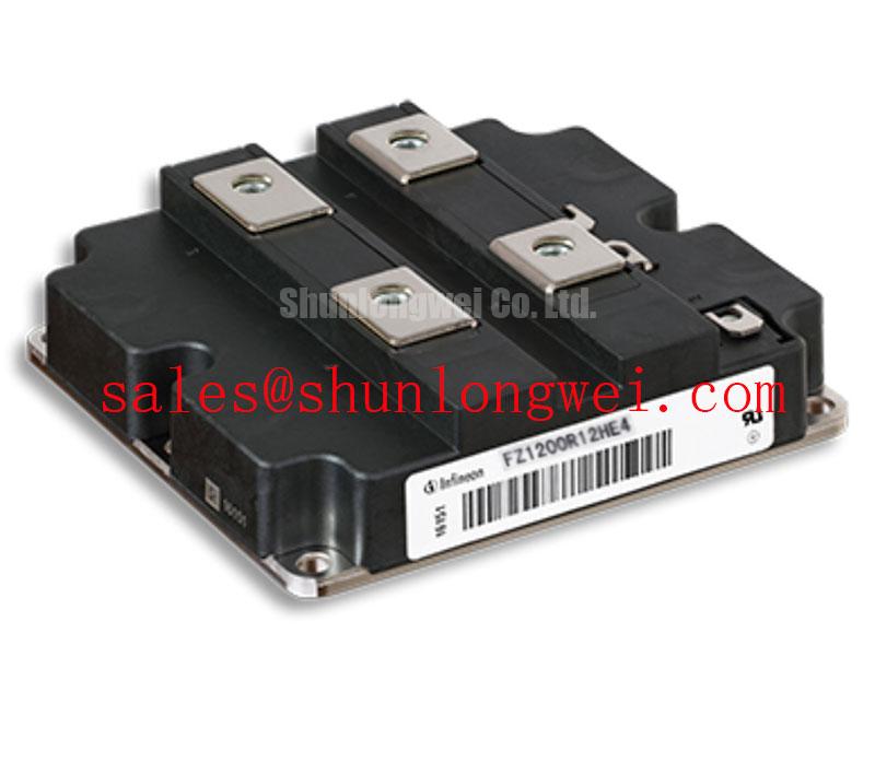
Identify the main load emitter terminal and the auxiliary Kelvin emitter return from the module markings and applicable connection documentation before tightening the driver wiring. The main emitter carries the power commutation current; the auxiliary return is intended to provide a cleaner reference for gate-control feedback when the package interface supports that topology. Treating both connections as interchangeable can defeat the purpose of the driver layout.
The power loop should use a short, low-inductance path between the module, DC-link structure, and switching load. The gate loop should remain physically independent from that path and return to the driver through the auxiliary emitter connection. In a laminated busbar arrangement, keep the gate-drive wiring outside the principal high-current field where practical, and avoid placing the driver reference conductor across a busbar joint or a high-current terminal transition.
Gate-driver sourcing and sinking capability must be selected against the actual gate charge, switching frequency, gate resistance, and required transition time of the complete circuit. The driver must control both turn-on and turn-off currents without entering an unstable operating condition. External gate resistance is a tuning element: increasing it can reduce edge speed and ringing, while reducing it can increase switching stress and parasitic oscillation. The correct value is system-determined and should be established from measured gate and collector-emitter waveforms.
A practical bench sequence is to begin with the proven driver arrangement used by the original inverter, confirm the polarity and continuity of each gate path, and then compare the auxiliary-return waveform with the controller reference. If the gate signal is clean at the driver but distorted at the module, inspect connector contact pressure, cable routing, return separation, and the physical position of the damping resistor. If a replacement gate driver is being evaluated, the adjacent topology may include a rectification or supply-stage device such as BSM100GAL120DN2; its electrical role should be assessed separately from the FZ1200R12HP4 switching path.
The FZ1200R12HP4 is specified here as a Module with a rated voltage of 1200.0 V and rated current of 1200.0 A. Those values identify the component class and rating boundary, but they do not define the permissible operating point for a particular inverter. Switching frequency, junction temperature, cooling arrangement, commutation stray inductance, duty cycle, and protection coordination remain system-level design variables.
⚠️ Field Alert: Isolate the DC link and confirm discharge before touching gate, emitter, or power-terminal wiring, then apply the fastening method specified for the actual hardware rather than relying on visual tightness.
FZ1200R12HP4 Circuit Protection & Reliability: Calibrating High-Altitude Cosmic Ray Induced SEB Failure
Separate high-altitude single-event reliability analysis from routine module troubleshooting by first recording the installation altitude, DC-link operating voltage, switching waveform, and protection response. Terrestrial neutron flux can vary with altitude, and single-event burnout assessment depends on semiconductor construction, applied electric-field conditions, exposure environment, and the protection system. A specific FIT value or SEB probability cannot be assigned from the product name and nominal ratings alone.
For equipment evaluated near or above elevated terrestrial sites, the design team should examine the DC-link voltage headroom against the module’s rated 1200.0 V boundary and against measured transient peaks. This is a Design Consideration, not a manufacturer-certified altitude derating curve for this listing. The appropriate engineering task is to establish a validated voltage envelope using the applicable device documentation, environmental requirements, and switching test data.
During field diagnosis, inspect the event record before removing the module. Record whether the failure occurred during energization, regenerative operation, a line disturbance, a gate-drive fault, or a protection trip. Check the DC-link capture, gate-to-emitter waveform, clamp response, and fuse interruption timing where those records are available. A punctured device can be associated with several electrical stresses, so the failed part should not be assigned a single-cause explanation without correlating the surrounding measurements.
Layout remains important because parasitic inductance can convert a fast current transition into a local voltage overshoot. Minimize the commutation loop area, keep the DC-link decoupling physically close to the switching path, and inspect busbar joints for loose interfaces or unexpected current detours. The switching-node clearance and insulation system should be reviewed as a complete assembly, especially where altitude changes the surrounding insulation environment.
For background on Infineon power semiconductor families, engineers can consult the Infineon IGBT Modules & Discretes Official Portfolio. The Infineon EasyPACK™ reference describes a separate product family and should not be treated as a direct specification source for the FZ1200R12HP4.
FZ1200R12HP4 Operational Boundaries: Evaluating Short-Circuit Energy Let-Through Matching Limits
Coordinate the semiconductor fuse, gate-driver protection, current-detection circuit, and DC-link structure as one interruption chain before placing the FZ1200R12HP4 into a high-power converter. Fuse total clearing energy and module short-circuit withstand are related but different quantities. The fuse must interrupt the fault within the available electrical time window, while the module and its connections must survive the current and thermal stress that occurs before interruption.
Review the fuse manufacturer’s published total clearing I²t under the actual prospective fault current, DC voltage, circuit power factor, and installation arrangement. Then use that result, together with the applicable module short-circuit and transient limits from the device documentation, to evaluate coordination. The comparison must include wiring inductance, fuse lead length, current-sharing behavior, gate shutdown delay, and the response of any desaturation or overcurrent protection. A nominal fuse current label is not enough to establish coordination.
For a utility-scale 1500V central photovoltaic inverter, the system topology deserves particular scrutiny because a 1200.0 V module rating is not automatically equivalent to a 1500V DC-link operating allowance. Designers should verify the actual voltage applied to the module, switching transients, series or multilevel arrangement, and protection margin during commissioning. The inverter manufacturer’s topology and the module’s documented operating limits govern the final compatibility decision.
On a replacement job, compare the original busbar geometry, gate-driver timing, current sensor position, fuse class, and cooling interface before changing only the semiconductor module. The neutral evaluation of a related Infineon module, such as FZ1200R17KF6-B2, still requires a complete mechanical, electrical, thermal, and protection comparison; a different voltage or current rating does not by itself establish direct interchangeability.
After assembly, use a controlled low-energy test to verify gate polarity, auxiliary-emitter reference behavior, current-sensor direction, and protection-trip sequencing. Progressively review the switching-node waveform, DC-link response, and fault-interruption behavior under the system’s approved test procedure. The Unlocking Efficiency in Industrial Drives technical resource can provide additional context for evaluating switching behavior and power-stage architecture, while the final acceptance criteria remain specific to the completed inverter.