Content last revised on October 21, 2026
Assembly Integrity & Layout Architecture: Implementing Gate Drive Resistance Calibration for FZ600R12KE3S Replacement
With the DC link discharged and its isolation verified, identify the collector, emitter, and gate connections from the terminal drawing before placing meter probes on the FZ600R12KE3S. Record cold-state readings with the gate held at emitter potential using an approved handling fixture; an uncontrolled gate charge can make repeated measurements misleading.
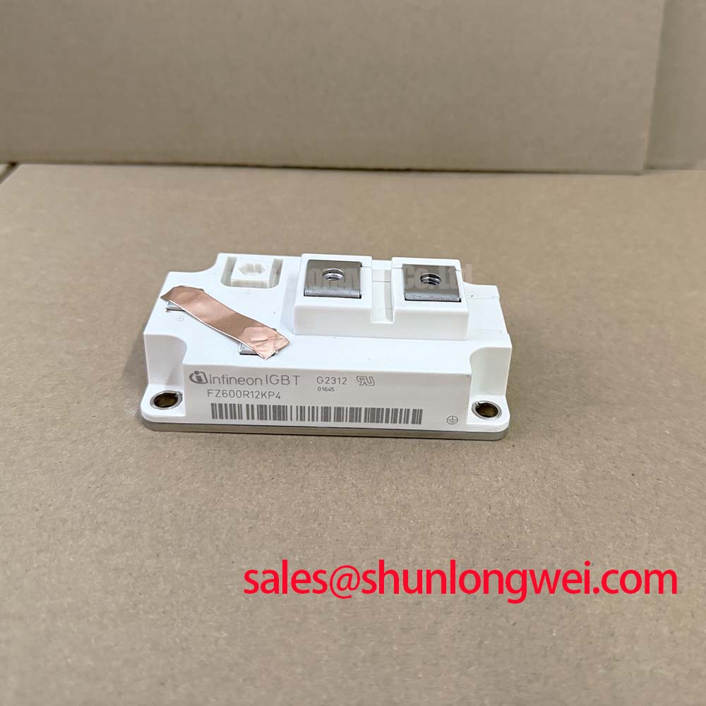
The Infineon FZ600R12KE3S is an IGBT Module with a 1200 V voltage rating and a 600 A current rating under the specified conditions. These are device ratings, not bench-test setpoints. For incoming inspection, retain the matching terminal drawing, rating conditions, and mechanical instructions alongside the measurement record.
Separate the external turn-on and turn-off gate-resistance paths on the legacy driver schematic before evaluating a replacement FZ600R12KE3S. As a Design Consideration, changing either path affects switching speed, driver loading, and transient behavior; resistor selection should follow measured switching performance rather than the resistance fitted to another module.
Trace the gate return independently of the high-current emitter connection wherever the documented terminal arrangement supports that routing. Do not assign an auxiliary terminal a Kelvin-emitter function without checking its designation. Keep the drive loop compact and preserve the equipment’s required clearance and creepage distances around power conductors. Gate-emitter voltage should be measured at the module connections, since a waveform captured only at the driver can conceal interconnect effects.
During controlled switching evaluation, compare gate ringing, collector-voltage overshoot, and switching energy under the same operating conditions. Miller-region behavior depends on gate charge, driver impedance, and collector-voltage transition; reverse-transfer capacitance is not itself a Miller-charge specification. Active clamping, if present, should be assessed together with driver protection timing rather than treated as permission to exceed the voltage rating.
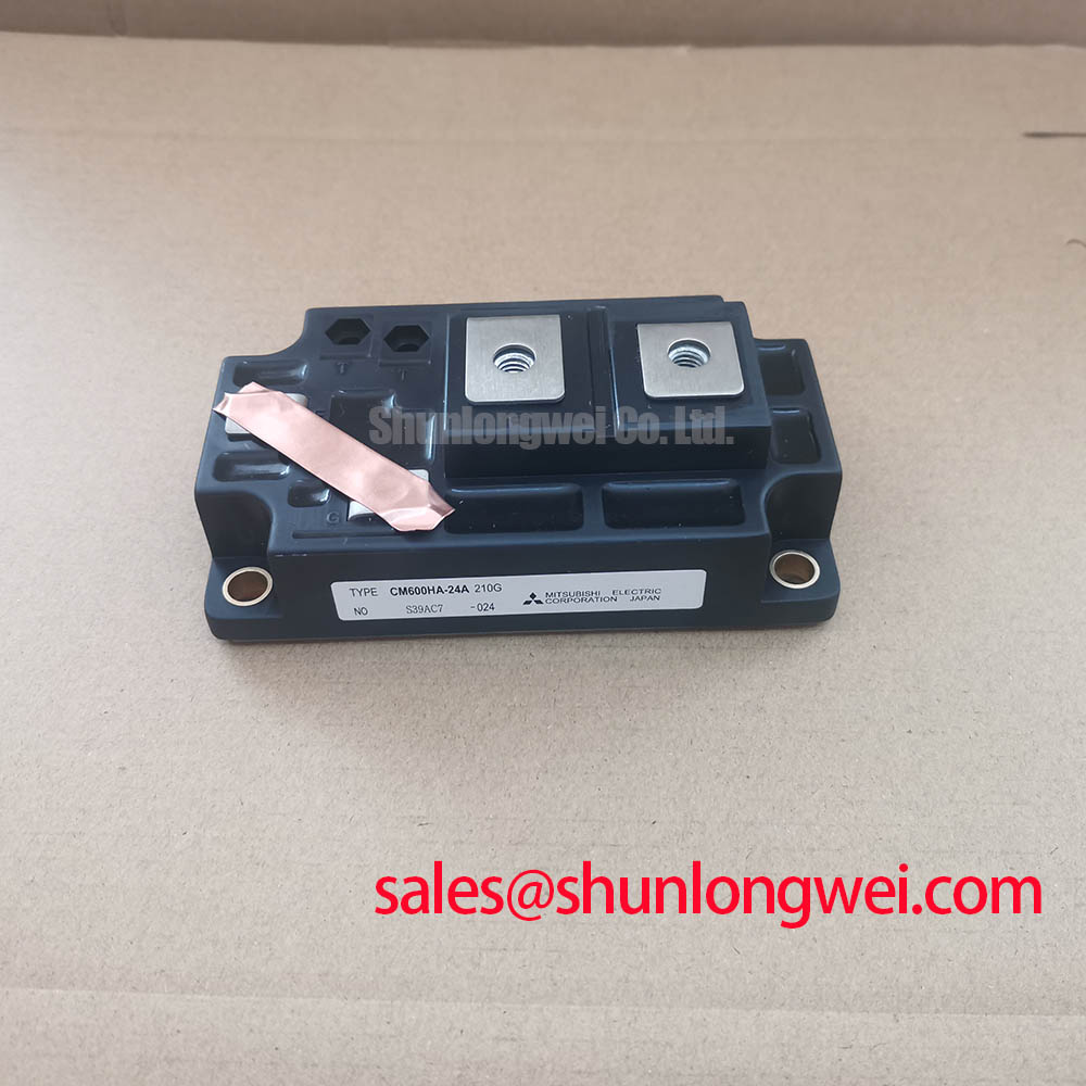
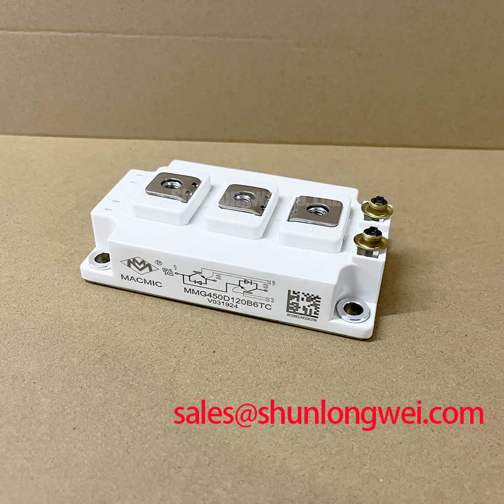
A comparison with FF600R12KE4 belongs in a documented compatibility review, not a presumed interchangeability list. Check circuit configuration, terminal positions, mounting geometry, and dynamic characteristics against the original design.
Benchtop Waveform Tuning: Mitigating Stress via Baseplate Convexity Inspection on FZ600R12KE3S
Inspect the mounting face and heatsink contact area for contamination, burrs, and uneven contact before interpreting temperature-dependent waveform changes. As a Design Consideration, mounting-face profile must be assessed against the manufacturer’s mechanical instructions; apparent convexity should not automatically be classified as damage or corrected by machining.
Apply the specified thermal interface material using the approved assembly procedure. Its distribution depends on surface profile, application method, and clamping pressure, so a generic film thickness is not an acceptance criterion for this module. Use a calibrated torque tool and the prescribed tightening sequence, supporting the module so that terminal connections do not impose additional bending loads.
Thermal settling matters when comparing switching captures. Record case temperature, cooling conditions, and operating duty with each measurement so that an apparent improvement in switching loss is not simply a different starting temperature. Where an upstream phase-controlled rectifier is present, distinguish its conduction-angle effects and line-frequency DC-link ripple from the module’s switching transients.
RC snubber assessment should follow the measured ringing frequency, damping, and component dissipation. Changing snubber components cannot compensate for poor thermal contact or excessive commutation-loop inductance. If the wider converter includes FF600R12ME4P_B11, assess its actual circuit role separately; the part number alone does not identify a rectifier stage or establish compatibility.
Benchtop Waveform Tuning: Mitigating Bolted Contact Oxidation on FZ600R12KE3S
Measure bolted power-joint resistance with a four-wire micro-ohmmeter, placing the sense probes so the intended interface—not an arbitrary length of busbar—is included. As an Engineering Recommendation, document probe positions, joint temperature, and instrument compensation before comparing readings with an approved assembly baseline.
Surface contamination, loose hardware, conductor strain, and contact deterioration can all influence a reading. Inspect the mating surfaces using the approved service procedure rather than aggressively abrading terminal finishes. No universal micro-ohm limit should replace the equipment manufacturer’s joint acceptance criteria.
💡 Bench Tip: Use ESD-controlled handling and compare cold-state diode-mode readings with a known-good reference under matching conditions, never with an energized assembly.
Where the documented circuit provides a diode path, check both probe polarities and account for parallel components before interpreting the result. A handheld meter can reveal an unexpected conduction path, but it does not establish high-current forward characteristics, reverse-recovery softness, or blocking capability.
After reassembly, compare thermal images under matched loading and cooling conditions. Reflective terminal surfaces can distort apparent temperature, so corroborate unusual patterns with suitable measurements. For switching-related ringing, inspect the laminated-busbar current loop and the diode commutation path together. Reverse-recovery behavior can influence electromagnetic emissions, but neither a diode-mode result nor a module rating establishes equipment-level EMC compliance.
FZ600R12KE3S Circuit Protection & Reliability: Calibrating Thermal Time Constants and Assessing Peak Junction Temperature
Build the overload assessment from the actual loss waveform and the manufacturer’s transient junction-to-case thermal data. As an Engineering Calculation method, convolve time-dependent power loss with the thermal impulse response; for a constant-power pulse, the junction-temperature rise follows pulse power multiplied by the applicable transient thermal impedance.
A multi-RC representation should reproduce that thermal response over the relevant pulse durations. Keep junction-to-case modeling distinct from the heatsink and coolant boundary conditions, and do not transfer fitted coefficients between different module types. Repetitive pulses also require the residual temperature from preceding pulses to be included.
For a potential high-speed rail or heavy-freight locomotive traction-inverter replacement, engineers should evaluate the complete duty profile and equipment qualification requirements. A regenerative-braking chopper assessment must include both semiconductor losses and the braking resistor’s energy-absorption capability. In bidirectional battery-converter evaluations, charging and discharging transitions should be included when reviewing temperature swings, without translating those swings into an unsupported service-life prediction.
The Infineon IGBT Modules & Discretes Official Portfolio provides manufacturer context for device selection. The Wide Bandgap Revolution discussion offers background when comparing switching technologies, not a test standard for this silicon IGBT module.
Before release, reconcile measured switching peaks and calculated junction-temperature excursions with the applicable device limits. Separately check the specified terminal-to-baseplate insulation test conditions against the equipment’s approved test procedure; the 1200 V semiconductor blocking rating is not an insulation withstand-test voltage.