Content last revised on October 4, 2026
FZ1200R12KL4C Module Overview
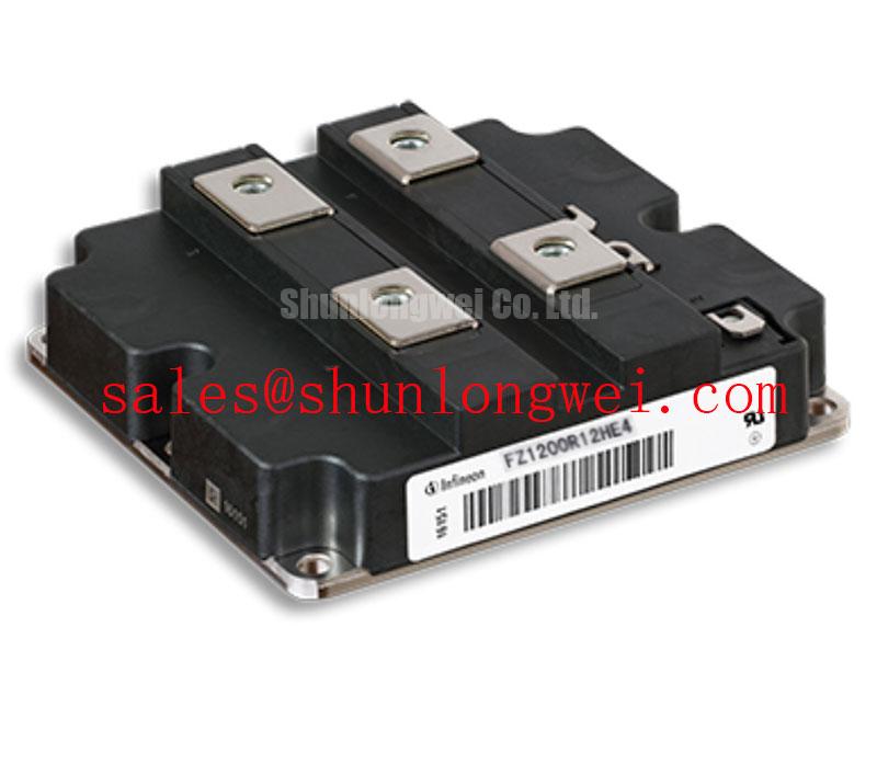
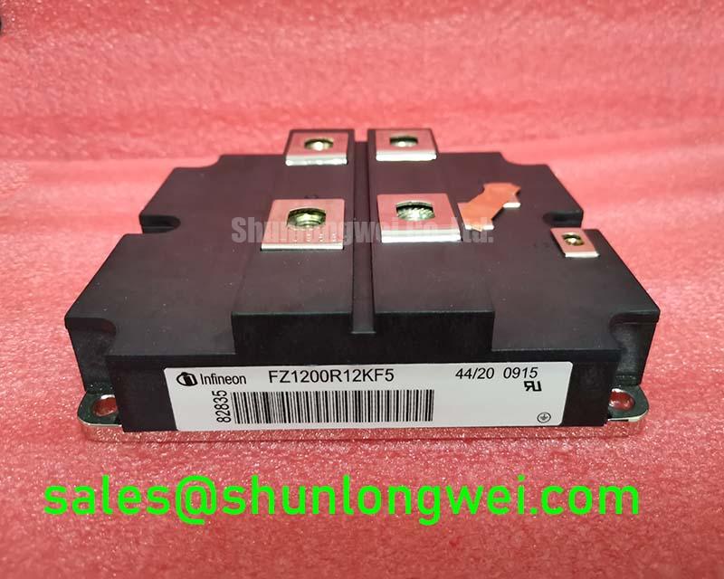
Before energizing a replacement assembly, verify the nameplate boundary, inspect the module body and terminals, and record cold-state resistance readings against a known-good reference circuit. The FZ1200R12KL4C is an Infineon IGBT module with an official rated voltage of 1200.0 V, an official rated current of 1200.0 A, and a Module package designation. These figures identify the device class, but they do not replace the original equipment manufacturer’s switching, cooling, insulation, and protection limits.
| Parameter | Official Specification |
|---|---|
| Manufacturer | Infineon |
| Part number | FZ1200R12KL4C |
| Rated voltage | 1200.0 V |
| Rated current | 1200.0 A |
| Package | Module |
| Product category | IGBT Module |
For maintenance teams evaluating a traction inverter, industrial converter, or another high-power switching platform, the correct decision starts with system compatibility. Confirm the original schematic, terminal assignment, gate-driver interface, cooling arrangement, switching frequency, protection thresholds, and mechanical envelope before installation. The values listed above are official product data supplied for identification; application limits remain dependent on the complete electrical and thermal design.
FZ1200R12KL4C Circuit Protection & Reliability: Calibrating Suppression of 2x VDC Voltage Doubling
Long motor leads can behave as a transmission-line structure rather than a simple conductor. During a fast switching transition, cable impedance, termination conditions, stray inductance, and motor-side reflections can combine to produce terminal overshoot that approaches a substantial multiple of the DC-link voltage. A two-times VDC observation should therefore be treated as a system-level switching event to investigate, not as an automatic withstand claim for the FZ1200R12KL4C.
Design Consideration: Begin with a controlled oscilloscope measurement at the module-side switching node and, where practical, at the motor terminals. Use a probe arrangement suitable for high common-mode voltage and keep the measurement loop physically compact. Compare the captured peak voltage with the DC-link voltage, switching state, motor-cable length, cable arrangement, and load condition. The engineering team should verify the actual peak margin against the official device voltage rating and the inverter’s protection coordination.
Output filters, common-mode elements, and differential chokes should be selected from measured impedance and switching behavior rather than from cable length alone. Their parasitic capacitance and inductance can affect gate-drive stability, common-mode current, conducted emissions, and turn-off stress. Designers should evaluate the complete filter and cable network with the inverter’s switching waveform, then validate the result during controlled high-load tests. No particular filter value can be assigned from the module rating alone.
Clearance and creepage must be checked around the complete DC-link, phase-output, and gate-drive structure. The required distance depends on working voltage, pollution environment, altitude, insulation material, and the applicable equipment standard. Keep high-voltage switching paths physically separated from low-level gate and feedback wiring, and confirm that busbar edges, fasteners, shields, and cable screens cannot reduce the intended insulation path.
For a traction inverter evaluation, the Infineon PrimePACK™ reference family provides useful industry context for high-power IGBT module integration, while the exact mechanical and electrical data for this part must be confirmed from the applicable device documentation. Engineers may also assess the related FZ800R12KS4_B2 as a separate IGBT module option in a converter design, subject to the original circuit requirements.
FZ1200R12KL4C Circuit Protection & Reliability: Calibrating the Junction-to-Case Thermal Network Simulation
Thermal verification should begin with the real switching profile rather than the headline current rating. A 1200.0 A official rating does not indicate that the module can carry that current continuously in every enclosure, cooling arrangement, pulse duration, or ambient condition. The maintenance engineer should collect load current, switching duty, heatsink temperature, coolant or airflow condition, and the duration of overload pulses before building a thermal model.
A transient thermal network can represent the junction-to-case response using several resistance and capacitance sections. In practical work, the model is driven by the measured or calculated semiconductor power waveform, and the resulting junction temperature is compared with the permitted device and system limits. The calculation should include conduction loss, switching loss, pulse repetition, case temperature, interface resistance, and the transient response of the heatsink. These are engineering calculations, not official specifications of the part unless stated in the manufacturer’s documentation.
During a field inspection, check the heatsink contact surface for contamination, uneven pressure, degraded thermal interface material, and signs of local discoloration. Confirm that the cooling path is not restricted by dust, collapsed filters, loose ducting, or fan imbalance. Where liquid cooling is used, inspect the approved flow path and look for evidence of leakage or condensation risk. A temperature rise at one terminal or one section of the busbar should be compared with phase loading and contact resistance before drawing a failure conclusion.
Terminal identification must be verified from the original mechanical drawing and circuit schematic. Do not infer gate, emitter, collector, auxiliary, or temperature-sense connections from physical proximity. With the equipment isolated and safely discharged, use continuity and insulation checks appropriate to the assembly, then compare each result with the known-good phase path. Any abnormal reading should be investigated with the driver disconnected where the service procedure permits, because surrounding capacitors, snubbers, and semiconductor paths can influence a cold-state measurement.
Vibration-proof busbar fastening is a system responsibility. Inspect the approved hardware, joint surfaces, support points, and strain relief, then apply the equipment manufacturer’s specified tightening procedure. A loose or mechanically stressed connection can create localized heating and intermittent switching behavior, while excessive force can damage the module interface or distort the busbar. Keep the module’s thermal interface uniform and avoid loading the terminals with unsupported cable or laminated busbar weight.
⚠️ Maintenance Note: During scheduled service, monitor contact and heatsink temperature trends while checking the cooling path for dust accumulation, because a clean-looking module can still have deteriorated thermal contact or restricted airflow.
For thermal architecture studies involving insulated substrates and advanced cooling arrangements, the practical reference The Advanced Thermal Management Revolution can support broader maintenance planning. It should not be treated as a substitute for the thermal impedance data and mounting instructions applicable to the FZ1200R12KL4C installation.
FZ1200R12KL4C Circuit Protection & Reliability: Calibrating High dv/dt Cross-Conduction Shoot-Through
High dv/dt at the switching node can couple through parasitic capacitances into the inactive gate circuit. The resulting gate disturbance may appear as unexplained current overlap, excessive turn-off loss, waveform asymmetry, or repeated protection trips. These symptoms do not identify one single failed component. The correct investigation compares the high-side and low-side gate signals, driver supply behavior, emitter reference, dead-time implementation, and switching-node waveform under the same operating condition.
Design Consideration: Minimize the shared impedance in the power commutation loop and keep the gate-driver return path referenced to the correct emitter point. Gate wiring should be short, physically controlled, and separated from high-current switching conductors. The final loop arrangement, gate resistance, clamp behavior, and protection timing must be determined by the system designer and verified with an appropriately rated differential probe.
An active Miller clamp can help hold the inactive gate at a controlled state during a high dv/dt transition when the driver architecture supports that function. A negative gate-bias strategy may also be considered, but the applicable voltage must come from the approved driver design and the device documentation. Do not impose a generic negative bias range on this module without confirming the gate-emitter absolute maximum rating, driver isolation, power-up behavior, and fault-state response.
When troubleshooting, first confirm that the driver supply does not collapse during the switching event. Next compare the command signal at the controller with the signal at the power-device gate, checking for propagation delay, ringing, excessive common-mode movement, and unintended overlap. If the gate waveform looks acceptable at the driver but abnormal at the module, inspect the physical gate loop, connector contacts, emitter reference, and local decoupling. If the waveform is abnormal at the driver output, investigate the driver, isolation barrier, protection logic, and control timing.
Protection coordination should include overcurrent detection, short-circuit response, desaturation or equivalent monitoring where provided by the system, soft shutdown behavior, and fault latching. The FZ1200R12KL4C rating alone does not confirm a particular short-circuit withstand time or switching frequency. Those values require the relevant official electrical and dynamic data, followed by controlled validation on the actual inverter platform.
For equipment used in high-speed rail or heavy freight locomotive traction inverter evaluation, vibration, temperature cycling, contamination, and cable movement can gradually change gate-loop conditions. Inspect connector retention, shield termination, busbar support, and the driver board mounting points whenever a fault appears only under acceleration, braking, or cabinet vibration. Correlate the event log with the measured gate and collector-emitter waveforms instead of assigning the fault solely to the power module.
Assembly Integrity & Layout Architecture: Implementing Multi-Module Parallel Current Sharing for FZ1200R12KL4C
Paralleling high-current IGBT modules requires electrical symmetry, thermal symmetry, and mechanical symmetry. The positive temperature coefficient commonly associated with steady-state conduction behavior can support static current balancing, but it does not guarantee equal dynamic current during turn-on and turn-off. Differences in gate-loop inductance, emitter path impedance, busbar geometry, driver delay, thermal coupling, and connector resistance can cause one module to switch earlier or carry a disproportionate transient.
Engineering Recommendation: Use a physically symmetrical power layout and provide each paralleled module with a closely matched gate-drive path. The system engineer should verify current sharing with current probes or suitable Rogowski measurements across the intended operating range, including cold start, thermal steady state, overload transition, regenerative operation, and fault response. The verification should include the collector-emitter voltage and gate-emitter waveform of each module, not only the combined phase current.
Shared gate-drive arrangements should be approached cautiously. A common driver can reduce component count, but it may also allow one module’s parasitic behavior to influence the others. Individual gate resistors, controlled return paths, and matched wiring can improve observability and adjustment, subject to the driver design and the module’s approved connection method. Designers should avoid assuming that equal wire length alone produces equal dynamic behavior; connector construction, bends, clamping, and busbar proximity also affect the circuit.
Thermal matching requires more than installing modules on the same heatsink. Check the flatness and cleanliness of each mounting surface, the consistency of the approved interface material, and the distribution of cooling flow or thermal mass. The junction-to-case and case-to-heatsink portions of the thermal path should be represented separately in the design calculation. If one parallel position runs hotter, inspect its electrical current share and mechanical interface before changing the control settings.
When comparing possible system configurations, the related FZ3600R12HP4 may be reviewed as a separate product option for its own documented voltage, current, package, and application conditions. It should not be treated as an automatic substitute for the FZ1200R12KL4C. Form-fit, gate-drive compatibility, thermal impedance, terminal arrangement, protection behavior, and qualification requirements must all be confirmed by the responsible design authority.
Before returning a repaired converter to service, inspect the complete commutation path, torque and support condition of the busbars, gate connector retention, cooling interface, insulation distances, and protective interlocks. Conduct low-energy functional checks before applying full DC-link voltage, then increase operating stress while recording switching waveforms, case temperatures, and phase-current balance. This staged validation gives the maintenance team evidence that the installed module and its surrounding architecture are operating within the verified system envelope.