



Content last revised on September 12, 2026
GD300HFX170C6S Operational Boundaries: Evaluating High dv/dt Cross-Conduction Shoot-Through Limits
| Specification | Value |
|---|---|
| Manufacturer | StarPower |
| Model | GD300HFX170C6S |
| Category | IGBT Module |
| Topology | Dual Half-Bridge Module |
| Rated Voltage | 1700 V |
| Rated Current | 300 A |
| Package | Power Module |
Measure the high-side and low-side gate-to-emitter waveforms at the module terminals while the inverter operates through the switching condition that produces the fault. A clean command signal at the driver board does not prove that the gate terminals see the same waveform, because common-emitter inductance, isolated-driver delay, busbar coupling, and power-loop dv/dt can alter the local voltage.
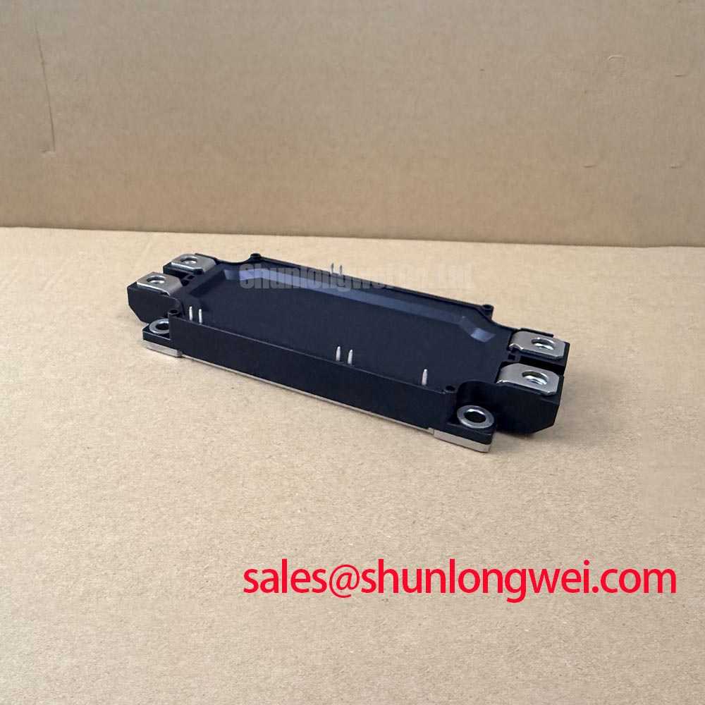
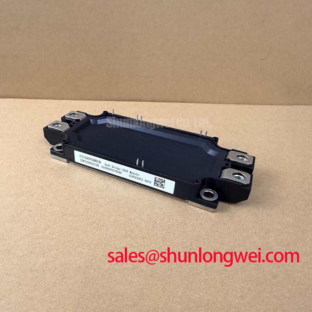
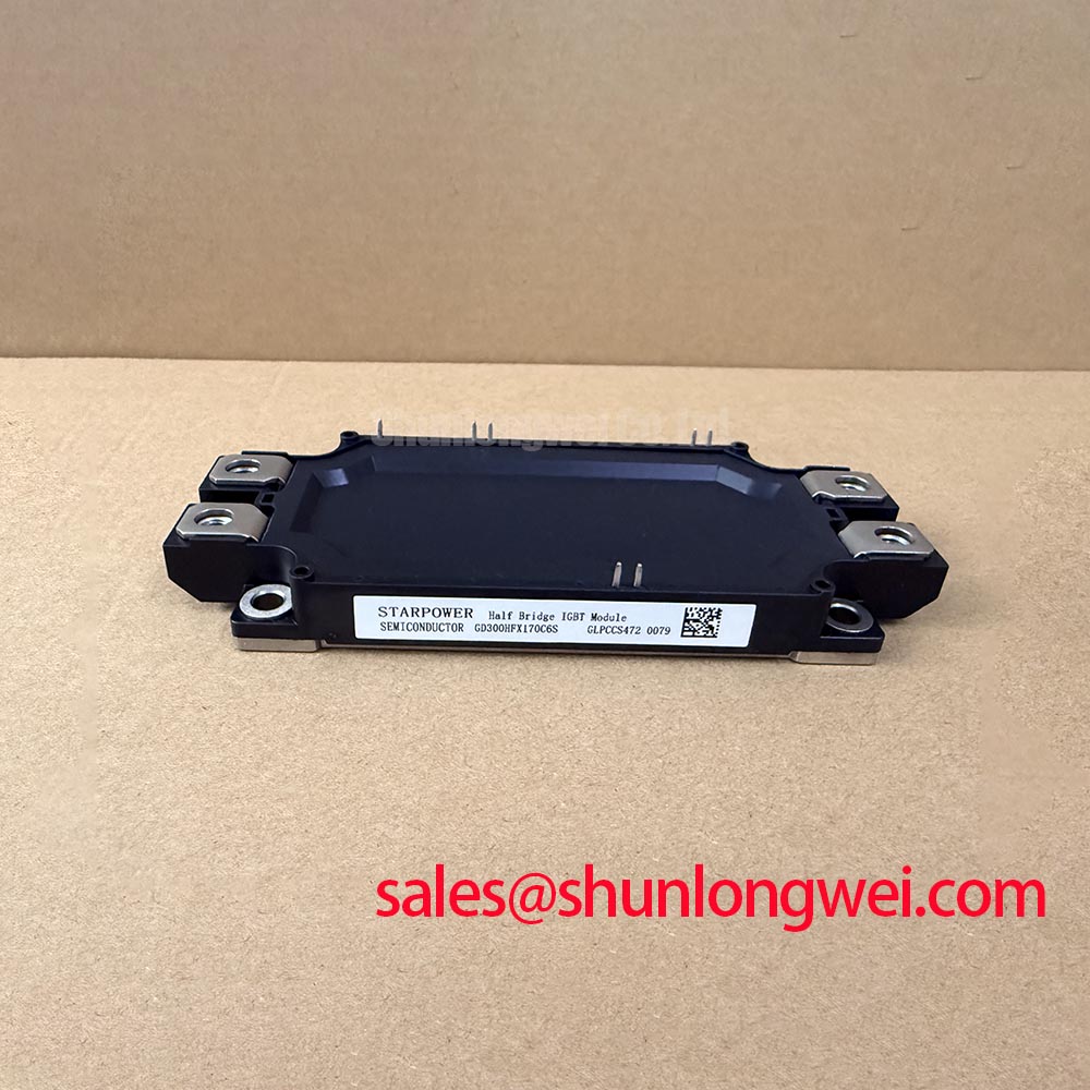
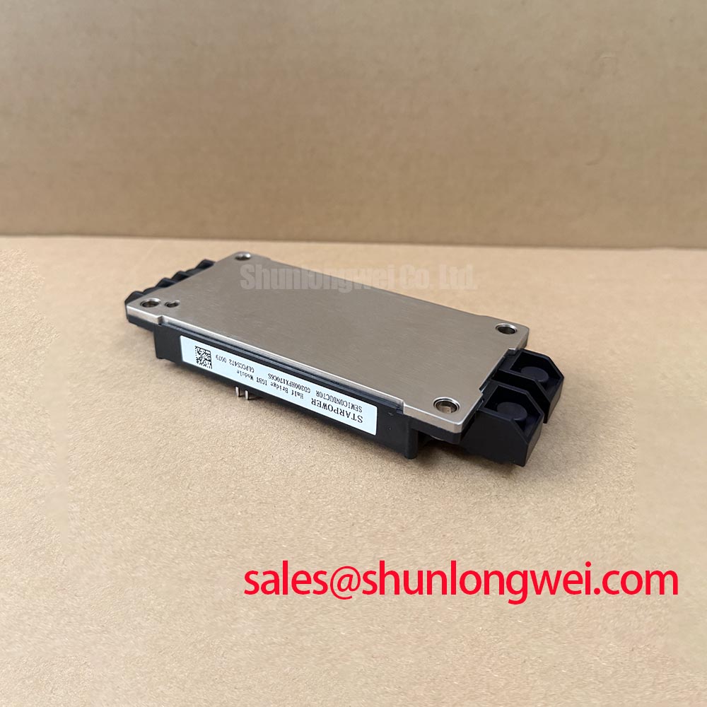
The GD300HFX170C6S is a 1700 V, 300 A StarPower IGBT module with a dual half-bridge topology. Its current and voltage ratings identify the device class, but they do not establish a universal switching frequency, gate resistance, dead time, short-circuit duration, or permissible transient profile for every converter. Those limits remain dependent on the original power-stage design, cooling arrangement, gate driver, DC-link construction, and switching test conditions.
For a high-power central photovoltaic inverter, begin by checking whether the upper and lower IGBT commands overlap at the driver outputs and then repeat the measurement directly across each gate-emitter pair. A false turn-on can be produced by a Miller current pulse during the opposite device's collector-emitter voltage transition. The diagnostic record should include gate voltage, collector-emitter voltage, phase current, and the timing relationship between the two commands. Compare the suspect phase with a known-good phase under the same operating point.
Long motor or inverter output cables can behave as transmission lines. Reflections at the remote load, cable termination, and local impedance can create a transient approaching twice the incident step under particular electrical conditions. A practical design consideration is to verify the far-end waveform rather than judging cable stress from the inverter-side probe alone. Common-mode chokes, dv/dt filters, termination methods, or other output-network components should be selected from the complete cable and load model, with the final peak voltage verified against the module's switching limits.
The gate driver should provide deliberate separation between turn-off and turn-on commands. Dead time must be established from measured driver delay, device turn-off behavior, temperature, current, and the worst-case tolerance stack, rather than copied from an unrelated module. A soft turn-off or controlled gate discharge can help limit overshoot during a fault, but the resulting collector-emitter stress and protection response require oscilloscope verification.
A low-impedance active Miller clamp is a design consideration when high dv/dt threatens to lift the inactive gate. Its effectiveness depends on the clamp connection, driver current capability, gate-loop inductance, and the location of the return path. Negative gate bias can also be evaluated for turn-off immunity, with the actual value determined by the driver and the manufacturer's gate-emitter limits. Do not assume that a negative bias used on another IGBT family is suitable for this module without checking the applicable gate ratings and transient behavior.
Keep the power commutation loop and gate loop physically separate, minimize shared return impedance, and route the gate and emitter paths as a tightly coupled pair. The driver reference should return to the module's intended emitter connection instead of travelling through a high-current busbar path. If a common-mode ground bounce appears on the measured gate waveform, repeat the test with a properly rated differential probe and a short connection arrangement before changing the gate network.
For snubber or MOV coordination, treat the MOV as one element in a layered overvoltage network rather than as a substitute for low-inductance layout. The DC-link clamp level, pulse energy, repetitive duty, wiring inductance, and device voltage margin must all be checked together. A MOV selection that appears suitable during a low-energy bench test may behave differently during repeated switching events in a utility-scale inverter.
Assembly Integrity & Layout Architecture: Implementing Cosmic Ray Robustness: Voltage Derating for GD300HFX170C6S
Record the actual DC-link voltage and switching overshoot at the module terminals during the highest-energy operating condition before assessing high-altitude voltage margin. The 1700 V rating of the GD300HFX170C6S is an official product parameter, while a safe operating margin for a particular solar inverter must be established from the switching waveform, environmental conditions, protection network, and applicable reliability evidence.
Terrestrial radiation effects, including neutron-related single-event stress, are system reliability topics that cannot be converted into a dependable FIT or SEB figure without a qualified device-specific test method, environmental model, voltage condition, and source data. No numerical failure rate or operating-life prediction should be assigned to this module from altitude alone. When equipment is installed above 2000 m, the engineering review should include the actual site altitude, insulation coordination, cooling performance, creepage and clearance requirements, DC-link control range, and transient records.
For a 1500 V photovoltaic central inverter, the nameplate bus voltage should not be treated as the only electrical stress. Switching overshoot, regenerative events, control faults, unequal module sharing, and surge-network tolerance can raise the instantaneous collector-emitter voltage. Designers should reduce parasitic loop inductance, coordinate active clamping with the DC-link protection system, and verify peak margins during representative switching tests. Any voltage derating policy should be based on documented reliability analysis rather than a generic percentage.
Parallel-module operation requires a symmetrical electrical and thermal arrangement. Use matched busbar geometry, equivalent current paths, and comparable gate-loop lengths so that one module does not receive a materially different commutation environment from its parallel devices. The positive temperature coefficient commonly associated with IGBT on-state voltage can support steady-state static current sharing, but it does not guarantee dynamic sharing during turn-on, turn-off, short-circuit protection, or unequal stray inductance.
Check each parallel branch under load by comparing collector-emitter voltage, gate-emitter voltage, current-probe data, and case or heatsink temperature. A current imbalance may arise from gate-driver mismatch, busbar asymmetry, thermal contact variation, measurement placement, or device parameter spread. Corrective work should address the measured mechanism, followed by a repeat test over the expected current and temperature range.
Clearance around the power terminals and busbars should be determined from the working voltage, transient environment, pollution level, altitude, insulation system, and applicable installation standard. The module's published voltage value is not a substitute for a complete creepage and clearance review inside the finished inverter. Avoid routing low-level control wiring through the electric-field region of the commutation loop, and provide a controlled shield or reference strategy where common-mode interference reaches sensors or isolated driver supplies.
Material selection also affects assembly robustness. Silicon nitride ceramic substrates are widely discussed for high thermal shock applications; the general material background can be reviewed through Silicon Nitride ceramic substrate information. Polyphenylene sulfide is also used in high-temperature engineering applications, with background available from Polyphenylene sulfide material information. These references describe material classes, not a confirmation of the internal construction of the GD300HFX170C6S.
For broader context on wide-bandgap switching behavior and its associated design challenges, the Wide Bandgap Revolution guide may help engineers compare system-level switching considerations. It should not be used to infer undocumented internal features or ratings for this silicon IGBT module.
GD300HFX170C6S Thermal-Electrical Optimization: Thermal Feedback Practical Tuning
Measure the temperature rise across the heatsink contact area and compare the current carried by each parallel path before changing gate-drive settings. A local hot region, unequal collector current, or different switching edge may point to an interaction between thermal impedance, busbar geometry, gate-loop parasitics, and assembly pressure rather than to a single component fault.
The official product data identifies the GD300HFX170C6S as a 300 A dual half-bridge power module. That rating must be evaluated with the complete thermal path, including the module mounting surface, thermal interface material, heatsink or cold plate, airflow or liquid flow, ambient temperature, and converter duty cycle. A current rating alone cannot define allowable continuous operation in a cabinet.
Positive temperature dependence of on-state voltage can help parallel IGBTs approach static current balance: a warmer device tends to develop a higher on-state voltage, which can shift some current toward cooler devices. This is a design consideration, not a replacement for measured matching. Dynamic current sharing is governed more strongly by gate timing, driver impedance, common-emitter inductance, collector stray inductance, and the physical symmetry of the power circuit.
Use equal-length gate and emitter conductors wherever the circuit places modules in parallel. Keep the driver return path away from high-current switching conductors, and damp ringing only after measuring the gate waveform at the module pins. A resistor value that suppresses oscillation in one branch can slow another branch or increase switching loss if the loop inductances are different. The tuning target should therefore include gate overshoot, turn-off behavior, switching loss, collector-emitter overshoot, and thermal balance.
When troubleshooting an inverter that trips intermittently, capture the event with adequate bandwidth and synchronized current measurement. Inspect whether the gate voltage becomes unstable during a high-current transition, whether the collector-emitter waveform contains repeated ringing, or whether the thermal drift occurs before the protection trip. Check the driver supply, isolation barrier behavior, gate resistor connections, emitter reference, and sensor ground separately. The waveform should be compared with the same point on a healthy phase before a replacement decision is made.
Cooling maintenance is part of electrical reliability. Inspect heatsink fins, filters, fans, liquid channels, and cabinet air paths for contamination or restricted flow, then compare operating temperatures under a repeatable load. Thermal compound that has dried, migrated, or been applied unevenly can increase contact resistance even when the module remains mechanically tight.
Maintenance Note: Monitor contact-temperature rise during scheduled service and verify the cooling path before reconnecting power after cleaning or mechanical work.
Assembly Integrity & Layout Architecture: Implementing Thermal Interface Material Thickness Uniformity for GD300HFX170C6S
Inspect the module base and heatsink contact surfaces for contamination, burrs, trapped particles, and visible curvature before applying thermal interface material. Thermal contact quality depends on surface condition, material uniformity, clamping sequence, and the complete mechanical stack; it cannot be confirmed from fastener tightness alone.
Thermal interface material should be applied as a continuous, even layer appropriate to the selected product and the measured surface condition. The assembly process should define a controlled thickness target based on the chosen TIM, surface flatness, compression behavior, and manufacturer instructions. Excess material can increase thermal resistance, while insufficient coverage can leave air gaps.
Baseplate curvature should be checked with an appropriate inspection method before installation. Do not use excessive screw force to compensate for a warped heatsink or module base. A rigid mounting surface, even contact pressure, and a controlled sequence help distribute the TIM without creating a high-pressure corner that distorts the package or pushes compound away from the active contact region.
Use the specified fasteners, washers, thread condition, and torque procedure for the mechanical assembly. Tighten progressively in a cross-pattern or other sequence defined by the mechanical design, allowing the base to settle evenly. Because the official data supplied for this product does not state a universal mounting torque, the final torque must come from the module documentation and heatsink assembly specification rather than a generic value.
After mounting, inspect for compound extrusion, uncovered areas, tilted hardware, and contact marks that indicate uneven compression. Where service procedures permit, a controlled witness inspection of the removed interface can help identify whether the material spread was uniform. Reapply TIM when the interface has been disturbed; do not reuse a contaminated or mechanically displaced layer.
Electrical and thermal checks should be performed together after assembly. Confirm that the power terminals remain mechanically secure, that the gate wiring has not been pulled or rerouted into the switching loop, and that the heatsink temperature rises evenly during a controlled commissioning test. In humid or seasonally cold installations, inspect for condensation around the module, busbars, driver board, and sensors before energization. Enclosure heating, drainage, insulation, and airflow should be selected from the site's environmental conditions.
For replacement planning, engineers comparing a dual half-bridge module with a different power-stage format can review the neutral reference for CM1000E4C-66R, then verify topology, voltage, current, mechanical envelope, gate requirements, and protection behavior against the original inverter documentation. The GD300HFX170C6S has no drop-in replacements specified in the supplied product data, so interchangeability should be established by the system designer through dimensional, electrical, thermal, and functional validation.