



Content last revised on October 6, 2026
Transient Dynamics & Electrical Design: Optimizing Gate Drive Loop Geometry to Prevent Turn-On in K229A08
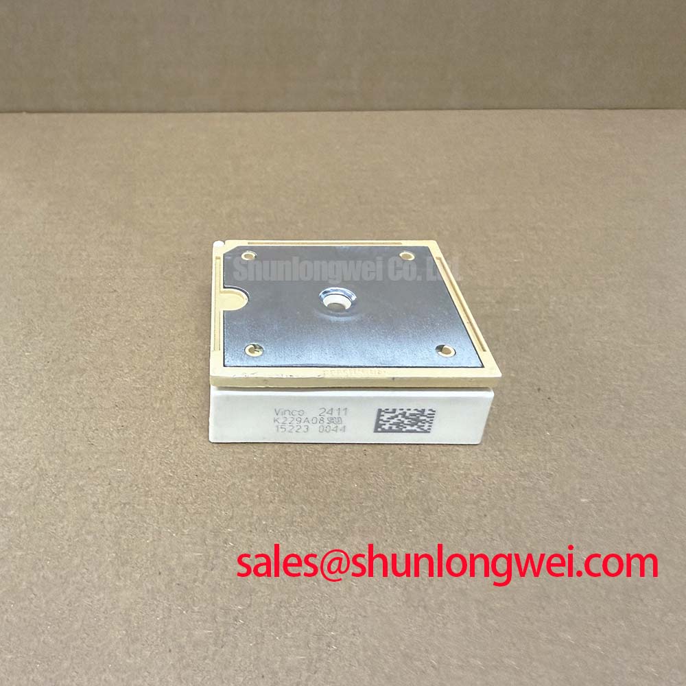
Before fitting K229A08 into an inverter, isolate the module, apply ESD precautions, inspect the terminals and housing, and record the cold-state resistance and diode-test readings against a known-good reference. Confirm the marked polarity and the original circuit position before connecting any gate-drive or power wiring. This Vincotech IGBT module combines an inverter stage with a rectifier section, so incoming inspection should evaluate both electrical paths rather than treating the part as a single transistor.
| Parameter | Symbol | Official Specification | Conditions |
|---|---|---|---|
| Inverter collector-emitter voltage | VCES | 1200 V | Tj = 25 °C |
| Inverter continuous collector current | IC | 25 A | Th = 80 °C |
| Inverter collector-emitter saturation voltage | VCE(sat) | 1.85 V typical | IC = 25 A, Tj = 125 °C |
| Rectifier repetitive peak reverse voltage | VRRM | 1600 V | Official Specification |
| Rectifier DC forward current | IF | 35 A | Th = 80 °C |
| Inverter thermal resistance | Rth(j-h) | < 1.03 K/W | Per IGBT |
| Maximum specified junction temperature | Tjmax | 150 °C | Official Specification |
The listed ratings are manufacturer data for the stated conditions, not a complete system operating prescription. Actual switching frequency, cooling arrangement, current waveform, gate-drive behavior, DC-link voltage, overload duration, and enclosure temperature must be verified by the equipment designer. The 1200 V inverter rating and 1600 V rectifier rating should be checked separately against the topology and transient environment of a commercial string inverter or micro-grid energy-storage converter.
💡 Bench Tip: Keep the device unpowered and at a stable laboratory temperature when comparing diode-mode readings, and use an ESD-controlled work surface so handling does not add a second fault variable.
Design Consideration: Gate-drive layout has a direct effect on the voltage seen between the gate and emitter during switching. The power emitter carries a rapidly changing current, while the gate driver needs a quiet reference. If the gate-return conductor shares a long section of high-current emitter copper, mutual inductance can introduce a transient error into the gate signal. That error may appear as ringing, delayed turn-off, or an unexpected rise in gate-emitter voltage during the opposite switch transition.
When integrating K229A08, designers should identify the gate terminal, the main power-emitter route, and any auxiliary emitter or driver-return terminal shown in the original module documentation. The driver return should follow the intended low-noise reference path back to the gate-drive circuit, while the high-current emitter connection should use a separate, short, low-impedance route. This separation reduces emitter mutual coupling and helps the driver measure the intended gate-emitter voltage instead of a combination of signal voltage and power-loop noise.
The commutation loop should be kept compact to reduce parasitic inductance and switching overshoot. This is a layout principle, not a guaranteed electrical limit for this module. The final board geometry depends on copper thickness, busbar construction, gate resistance, switching current, DC-link arrangement, and the measured waveform. During commissioning, observe the gate-emitter voltage and collector-emitter voltage simultaneously with suitable isolated or differential probes. A known-good switching waveform provides a more useful reference than a resistance measurement alone.
Oscillation should be investigated by checking probe grounding, gate-return routing, driver supply decoupling, and the physical distance between the driver and module. A waveform that changes significantly when the probe position changes may indicate measurement-loop pickup rather than a device defect. If the gate signal remains unstable with a controlled probing method, designers should evaluate gate resistance, clamp behavior, common-mode current, and the mechanical connection of the power terminals. The VCE(sat) value of 1.85 V typical at 25 A and 125 °C is a specified test condition and should not be used as a universal switching waveform target.
For cross-model evaluation, engineers may compare the electrical arrangement and thermal requirements of K420A4001, but a replacement decision requires confirmation of voltage, current, topology, terminal arrangement, thermal interface, and gate-drive compatibility. Similar application language does not establish interchangeability.
K229A08 Circuit Protection & Reliability: Calibrating Active Miller Clamp Implementation
Engineering Recommendation: An active Miller clamp can help limit unintended gate movement when the complementary switch experiences a high rate of collector-voltage change. The clamp should be placed according to the driver manufacturer’s application guidance and connected with a low-impedance path to the relevant emitter reference. Its effectiveness depends on propagation delay, gate-loop inductance, driver current capability, common-mode behavior, and the actual Miller charge of the assembled power stage. The K229A08 data supplied here does not specify a required clamp voltage, negative gate bias, or common-mode switching rate.
Some gate-drive architectures use a negative turn-off bias to improve immunity to parasitic turn-on. A value such as negative five to negative fifteen volts must not be treated as an official K229A08 requirement without the applicable module and driver documentation. The system integrator should verify the permitted gate-emitter voltage range, driver output capability, isolation behavior, and turn-off transient before applying any negative bias. Excessive gate stress can create a separate failure mechanism even when the clamp appears effective on the oscilloscope.
Short-circuit protection should coordinate the desaturation or VCE monitoring response with the module’s permitted short-circuit operating area and the complete protection delay. A soft turn-off strategy can reduce voltage overshoot by controlling the rate of current interruption, but its timing and gate-current profile must be validated on the assembled commutation loop. A bench test should capture the fault current, gate voltage, collector-emitter voltage, driver fault response, and DC-link condition as one time-correlated record.
High-speed semiconductor fuses require an I²t coordination study with the converter’s DC-link impedance and fault path. The fuse clearing characteristic, module short-circuit withstand capability, wiring inductance, and protection response time all contribute to the result. A fuse rating by itself does not demonstrate protection. Designers should use the relevant fuse manufacturer curves and the original K229A08 short-circuit data where available, then validate the arrangement under controlled fault-test procedures.
Rectifier protection also deserves separate attention. The official 1600 V VRRM and 35 A DC forward current at Th = 80 °C ratings apply to the rectifier section under their stated conditions. They do not automatically define permissible surge current, repetitive commutation stress, or line-side harmonic performance. Where a phase-controlled rectifier is used, the firing angle, line impedance, filter arrangement, and control strategy should be evaluated for current distortion and thermal loading rather than inferred from the nominal current rating.
⚠️ Field Alert: Never insert or remove a gate-drive connector while the DC link or auxiliary driver supply remains energized.
Transient Dynamics & Electrical Design: Galvanic Gate Drive Isolation, Reinforced on K229A08
Design Consideration: Galvanic isolation is a system property involving the isolator, PCB spacing, transformer or isolated power supply, connector arrangement, coating, contamination environment, and mechanical barriers. The available K229A08 specifications identify electrical and thermal ratings but do not certify a reinforced isolation barrier above 5 kV or a CMTI above 100 kV/µs. Those values must be selected and verified from the chosen gate-driver and isolated-power components, then assessed in the finished assembly.
For a commercial string inverter or micro-grid storage converter, the isolation boundary should be mapped from the controller domain to the high-side and low-side gate-drive domains. Keep primary-side control copper away from switching nodes, avoid routing sensitive communication traces alongside collector or DC-link conductors, and provide a deliberate return path for displacement current. Clearance and creepage are determined by working voltage, transient overvoltage, pollution environment, material group, altitude, and the applicable safety standard. The system designer must calculate the required distances from the certified equipment design rather than assign a generic value to the module.
Common-mode transient testing should be performed with the actual module, gate driver, isolated supply, bus structure, and intended load. Monitor both gate outputs while applying the expected switching conditions. A spurious pulse may result from insufficient isolator immunity, capacitive coupling across the isolation barrier, driver supply disturbance, probe reference error, or an unplanned return path through the heatsink. Comparing the affected channel with the known-good channel can narrow the search, but it does not replace an isolation and creepage review.
Gate-drive supply sequencing also requires verification. The controller should establish a defined off-state before the high-voltage bus is enabled, and the driver undervoltage behavior should be confirmed under startup, shutdown, brownout, and fault-reset conditions. If an isolated auxiliary supply has excessive ripple or slow recovery, the gate may not remain in the intended state even though the PWM command is inactive. The required supply voltage must be taken from the selected driver and the original equipment documentation, not guessed from the module part number.
For practical reliability work involving switching faults, thermal interfaces, terminal inspection, and waveform correlation, engineers can consult the Field Engineer’s Handbook. The guide should complement, not replace, the Vincotech documentation and the safety requirements governing the finished inverter.
EMI control is also a system-level task. A common-mode choke may reduce conducted common-mode current when selected for the actual spectrum and current waveform; background information is available in this reference on common-mode chokes. The choke cannot compensate for poor gate-loop geometry or an uncontrolled switching node. Any claim of CISPR or EN 55011 compliance must apply to the complete equipment after testing, not to K229A08 as an isolated component.
Preventing Spurious Faults: DC-Bus Operating Voltage Headroom Derating Guidelines for K229A08
Design Consideration: The inverter’s 1200 V VCES rating at Tj = 25 °C is a component boundary under the stated condition, not a recommended DC-bus operating voltage. Turn-off overshoot, stray inductance, control tolerance, temperature, load regeneration, and measurement uncertainty reduce usable voltage headroom. Designers should characterize the highest collector-emitter peak at the module terminals during the worst credible switching event and compare it with the applicable device limit.
Altitude and radiation-related reliability require source-specific analysis. Air insulation performance changes with atmospheric pressure, while terrestrial neutron exposure can vary with altitude and location. The supplied K229A08 data does not provide a Single Event Burnout cross-section, FIT rate, neutron susceptibility curve, or an altitude derating table. It would therefore be inappropriate to calculate a numerical SEB failure rate or claim a fixed voltage reduction for operation above 2000 m. Engineers evaluating high-altitude installations should obtain radiation data from the semiconductor manufacturer or an authoritative reliability study and combine it with the certified system insulation design.
The practical first step is to record the actual DC-link voltage, switching peak, ringing frequency, and temperature at the module terminals, not only at the capacitor bank. Differential probing should use a short connection method suitable for the voltage environment. Repeat the measurement during startup, maximum load, regeneration, line disturbance, and controlled shutdown. If the peak approaches the device boundary, reduce parasitic loop inductance, review switching speed, improve snubber placement, or revise the operating envelope as a system-level engineering decision. The correct intervention depends on the measured energy and the converter topology.
Thermal headroom must be assessed at the same time. The official inverter thermal resistance is less than 1.03 K/W per IGBT, and the maximum junction temperature is 150 °C. These figures do not establish the heatsink temperature, interface performance, airflow, or allowable continuous current in a finished product. The official 25 A continuous collector current at Th = 80 °C should be interpreted with the stated case-temperature condition and the real current waveform. Junction-temperature estimation should include conduction loss, switching loss, thermal interface behavior, and transient loading.
The rectifier path can create a separate DC-bus stress pattern, particularly when line commutation and energy-storage charging overlap. Check reverse-voltage peaks, forward-current heating, control timing, and any pre-charge or bypass contactor sequence. A Peltier or thermoelectric device is not a substitute for correctly sized power-stage cooling; general background on the Peltier effect and thermoelectric heat dissipation should not be interpreted as a K229A08 thermal specification.
During field diagnosis, compare the failed channel with an unaffected channel, inspect the gate waveform before removing the module, and document the DC-link condition at the moment of the fault where safe test procedures permit. A shorted inverter path may involve gate-drive malfunction, excessive transient voltage, thermal overstress, commutation error, insulation breakdown, or an external load fault. The measurement sequence should distinguish these possibilities without assigning a single cause from one symptom.