Content last revised on September 19, 2026
APT2X30D120J Thermal-Electrical Optimization: Baseplate Thermal Grease Layer Control Practical Tuning
Begin incoming inspection by isolating the APT2X30D120J from the equipment, reading the terminal markings against the original assembly documentation, and recording cold-state diode-mode and resistance readings before any powered test. This Microsemi unit is rated at 1200 V and 30 A as an Official Specification, with the supplied package designation listed as SP4 / SP6 Module. Those ratings establish the electrical identity to verify during service work; they do not establish an acceptable DC-link setting, gate-drive level, switching frequency, or cooling capacity for a particular inverter.
For a commercial string inverter or micro-grid energy-storage repair, first compare the removed module's terminal orientation, baseplate footprint, insulation arrangement, and mechanical clearance with the host equipment drawing. The system integrator should verify the original module documentation before interpreting any conduction path, because the supplied official information does not define the individual power-terminal mapping, auxiliary terminals, internal diode arrangement, or gate-emitter pinout.
Bench Tip: Establish cold-state readings on an ESD-controlled bench and compare them with a known-good circuit path only after confirming that stored DC-link energy has been discharged.
Thermal-interface work begins with a clean, visually inspected heatsink face and module baseplate. Remove residual compound without scratching either mating surface, inspect for raised debris around mounting locations, and check that the heat spreader does not rock when the module is placed dry. A rocking condition can concentrate mounting load and leave parts of the thermal interface poorly coupled, even where the compound appears evenly applied after removal.
For this 1200 V, 30 A IGBT module, thermal grease thickness is a Design Consideration, not an official APT2X30D120J parameter. A thin, continuous layer in the general range of 50 to 100 um is commonly evaluated where the mechanical flatness and grease specification support it. The objective is to fill surface asperities while avoiding a thick layer that becomes the dominant thermal resistance. The final process should be qualified by the equipment owner using its approved compound, surface-finish requirements, and measured operating temperatures.
Apply the module with controlled placement rather than sliding it through a long grease path. When multiple mounting screws are present, use a staged cross-pattern sequence so the baseplate settles progressively. Tightening one side fully before the others can distort the interface and make later temperature readings difficult to interpret. Actual screw size, torque, washer stack, and torque sequence must come from the module documentation and the equipment mechanical drawing; they are not confirmed by the available official data.
Field Alert: Do not power a converter after remounting until every power connection and every accessible gate-drive connection has been checked for correct seating and intended isolation.
When a repaired inverter reports a thermal-related fault, inspect the cooling path in layers: fan or pump operation, heatsink contamination, compound coverage, clamp pressure, and temperature-sensor placement. A rising temperature trend may involve any of these interfaces, as well as load conditions or switching behavior. Do not infer a module junction condition from a single external heatsink measurement. Compare measurements under a documented, repeatable load state and retain the results with the incoming inspection record.
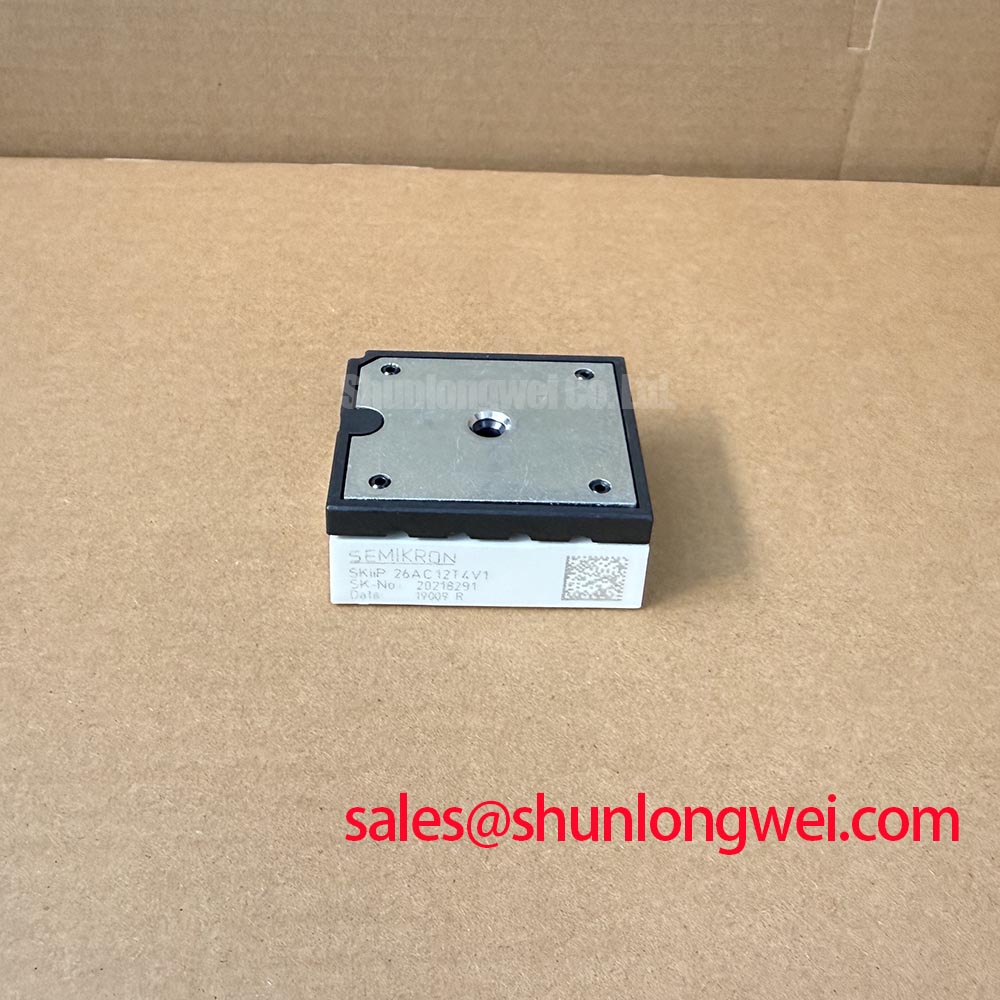
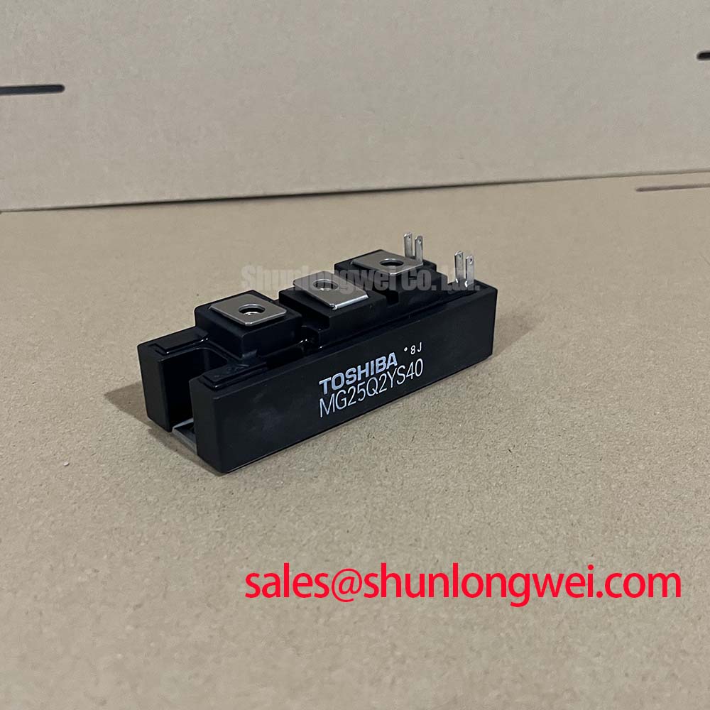
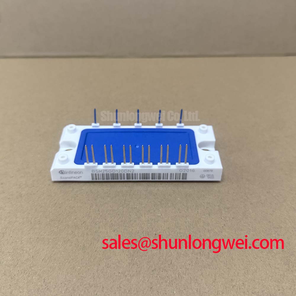
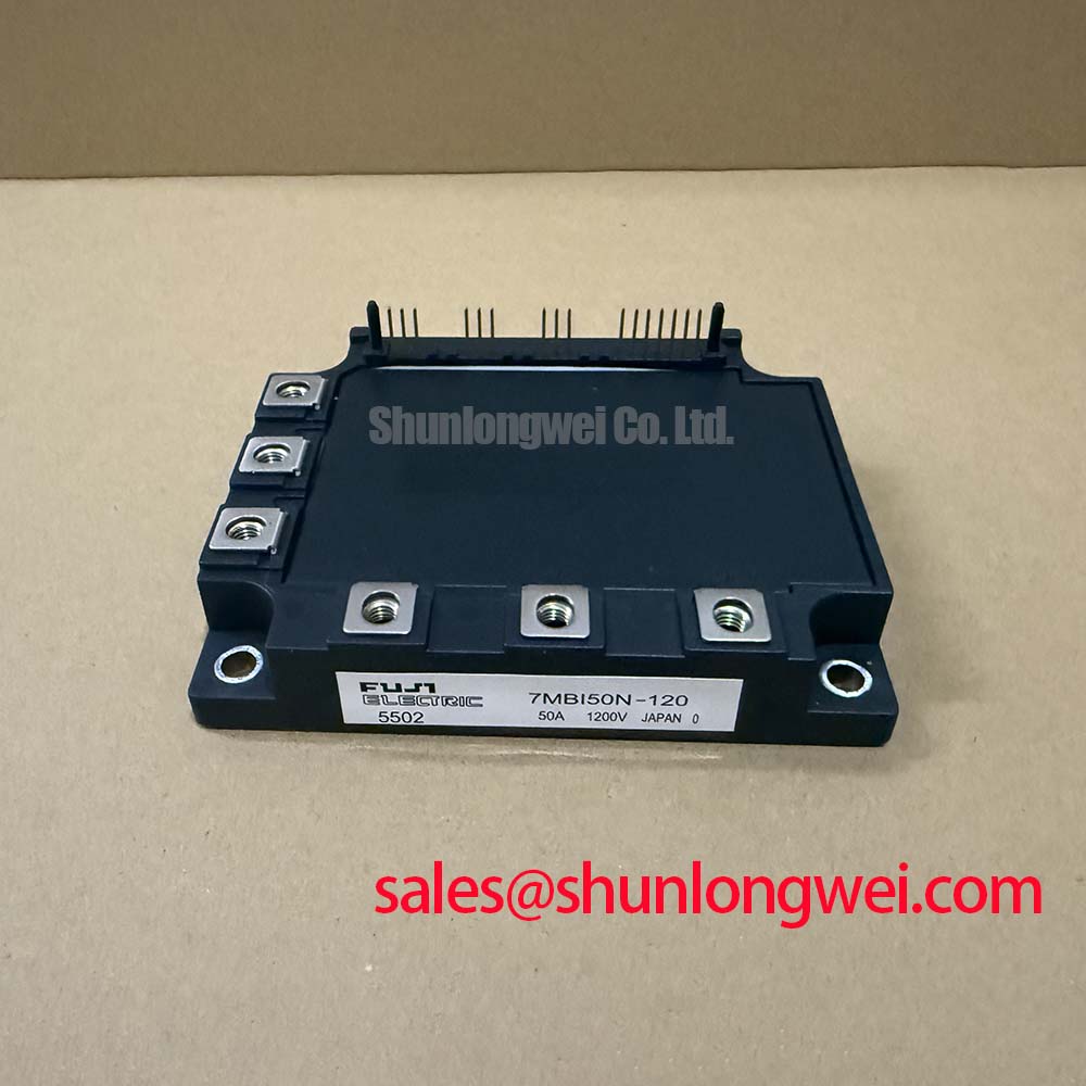
Where a replacement assessment is necessary, a linked GD15PJX120F4S listing can be reviewed as a separate candidate. Electrical ratings alone do not establish interchangeability. The repair engineer should verify terminal assignment, package dimensions, driver compatibility, insulation arrangement, protection thresholds, thermal interface, and the host controller's expected switching behavior before approving any alternative.
APT2X30D120J Thermal-Electrical Optimization: High-Altitude Cosmic Ray Induced SEB Failure Practical Tuning
The stated 1200 V rating is an Official Specification for the APT2X30D120J, but it is not a field failure-rate prediction. At elevated installation altitude, terrestrial neutron exposure and system voltage stress can be subjects for Design Consideration. No qualified FIT value, single-event burnout characterization, altitude derating curve, or approved DC-bus headroom rule is provided in the supplied official information. It would therefore be inappropriate to calculate a service-life value or claim a quantified SEB risk for this model.
For equipment that will operate above 2000 m, the responsible system engineer should review the original manufacturer documentation, applicable installation standard, enclosure conditions, actual DC-link waveform, protective response, and application-specific reliability assessment. This is especially relevant when the module is part of an energy-storage inverter with repeated high-energy switching events. The correct evidence is controlled test data or an authoritative manufacturer assessment, rather than an assumed multiplier derived from altitude alone.
Dead-time and complementary gate interlock are also system-determined controls. Their purpose is to prevent simultaneous commanded conduction in paired switching positions, but no valid numerical setting can be inferred from the module voltage and current ratings. During commissioning, verify the command relationship at the driver outputs and, where safely possible, inspect switching waveforms under controlled conditions. Unexpected current rise can result from timing overlap, driver-reference disturbance, unsuitable gate-loop routing, a damaged device, or a fault elsewhere in the power stage. A waveform review is more defensible than assigning one cause from a protection log.
The gate-return path should be deliberately separated from high-current power-return paths where the original module pin arrangement permits it. The available official data does not confirm a Kelvin-emitter auxiliary terminal on this model, so do not assume one exists. Verify the actual terminal function from the original module drawing. A low-noise driver reference helps the controller observe the gate-emitter voltage intended by its design rather than a voltage disturbed by power-loop current.
In a larger power train, the relationship between the inverter bridge, DC-link hardware, and upstream conversion stage should be checked as a topology question. A device such as FZ800R12KS4_B2 may be evaluated as a separate front-end or auxiliary-stage component reference, subject to the original schematic and its own documentation. It does not define a replacement or performance setting for the APT2X30D120J.
Preventing Spurious Faults: Negative Gate Bias vs Active Miller Clamping Guidelines for APT2X30D120J
Before changing any gate-drive hardware, confirm the static gate path with the module disconnected from the energized converter. Inspect gate and return conductors for damage, compare resistor locations with the approved board revision, and check that isolated-driver supply references are connected as intended. The supplied APT2X30D120J data does not specify recommended positive or negative gate voltage, gate resistance, threshold voltage, gate charge, or an active Miller-clamp requirement. Those values must not be assigned from a generic IGBT practice.
Negative gate bias and active Miller clamping are gate-drive options used in some converter designs to improve off-state gate control during rapid collector-voltage transitions. A negative bias can increase the off-state margin when supported by the driver and module limits. An active clamp can provide a low-impedance gate-emitter path after the gate has reached its off-state condition. Neither measure is automatically suitable for this module, and neither should be retrofitted without reviewing the gate-emitter absolute limits, driver isolation rating, protection behavior, and original circuit design.
When unwanted turn-on is suspected, capture the gate-emitter signal at the actual module reference point using an appropriately rated differential measurement method. Compare the commanded state, gate waveform, collector-emitter waveform, and phase current. A gate excursion may indicate coupling through the switching node, common-mode disturbance, measurement-reference error, gate-loop inductance, or a driver issue. Confirm the measurement setup against a known-good channel before altering components.
Industrial current feedback can affect fault interpretation but does not identify a module defect by itself. Isolated phase-current sensing may use signal conversion principles related to delta-sigma modulation, while other current-measurement arrangements can use magnetic sensing principles associated with giant magnetoresistance. The equipment schematic and approved sensor documentation remain the source for calibration, timing, and fault-threshold decisions.
Thyristor gate-trigger quantities such as IGT and VGT do not describe this IGBT module and should not be used to set its driver. Likewise, pulse-train triggering methods intended for thyristors are not a substitute for validating the IGBT gate-drive circuit. Keep the diagnosis tied to the actual module type, its confirmed terminal documentation, and the converter's approved gate-drive architecture.
Benchtop Waveform Tuning: Mitigating Stress via Planar Symmetrical Busbar Geometry: Achieving Results on APT2X30D120J
With the module mechanically secured and the terminal mapping verified, evaluate the commutation loop as a physical assembly. The measured voltage peak during switching is influenced by DC-link voltage plus the voltage developed across stray loop inductance as current changes. This engineering relationship explains why busbar geometry, capacitor placement, conductor overlap, and return-path symmetry deserve attention. The APT2X30D120J rating of 1200 V is the official device boundary; the system engineer must measure actual peak voltage against that boundary during validated switching tests.
A planar, closely coupled supply-and-return arrangement is a Design Consideration for reducing loop inductance and associated overshoot. Keep the current loop compact, avoid long separated conductor paths, and place the approved DC-link capacitors according to the original converter layout. Do not apply an assumed inductance target or snubber-capacitor value to this module. Parasitics depend on the physical busbar stack, cable routing, capacitor construction, switching current, driver behavior, and measurement method.
Snubber tuning should be performed only with a measured waveform and a clear understanding of the converter protection scheme. A change that reduces one ringing condition can alter switching loss, recovery behavior, common-mode noise, or driver stress elsewhere. Engineers should verify voltage peaks, current waveform shape, repetitive behavior, and protection response across the required operating range. The device itself cannot be represented as independently compliant with system-level EMC standards.
Use short, controlled probing connections and document their location. Long probe ground leads can create apparent ringing that is dominated by the test setup rather than the power loop. If waveform behavior changes after busbar work, repeat cold-state checks, inspect terminal torque according to the applicable mechanical documentation, and compare the driver waveform with the pre-change reference. For wider three-phase switching and long-term power-conversion context, review The 1200 V CoolSiC™ MOSFET Advantage in Three as background material; it does not alter the official specifications or integration requirements of the Microsemi APT2X30D120J.