


Content last revised on September 10, 2026
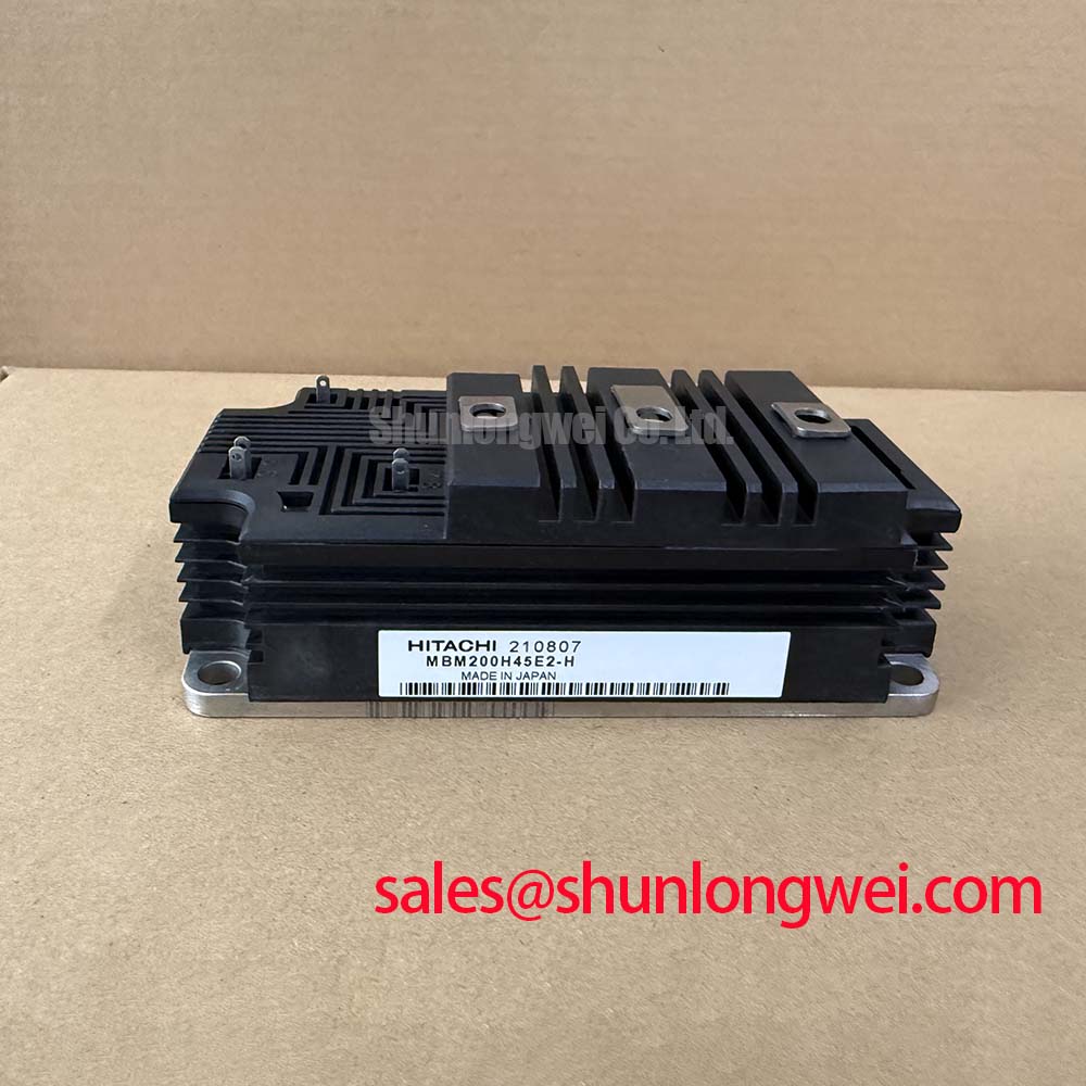
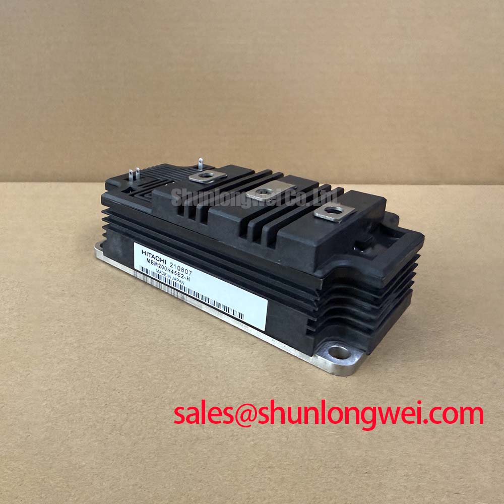
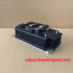
MBM200H45E2-H Hitachi 4500V 200A IGBT Module for High Voltage Inverters
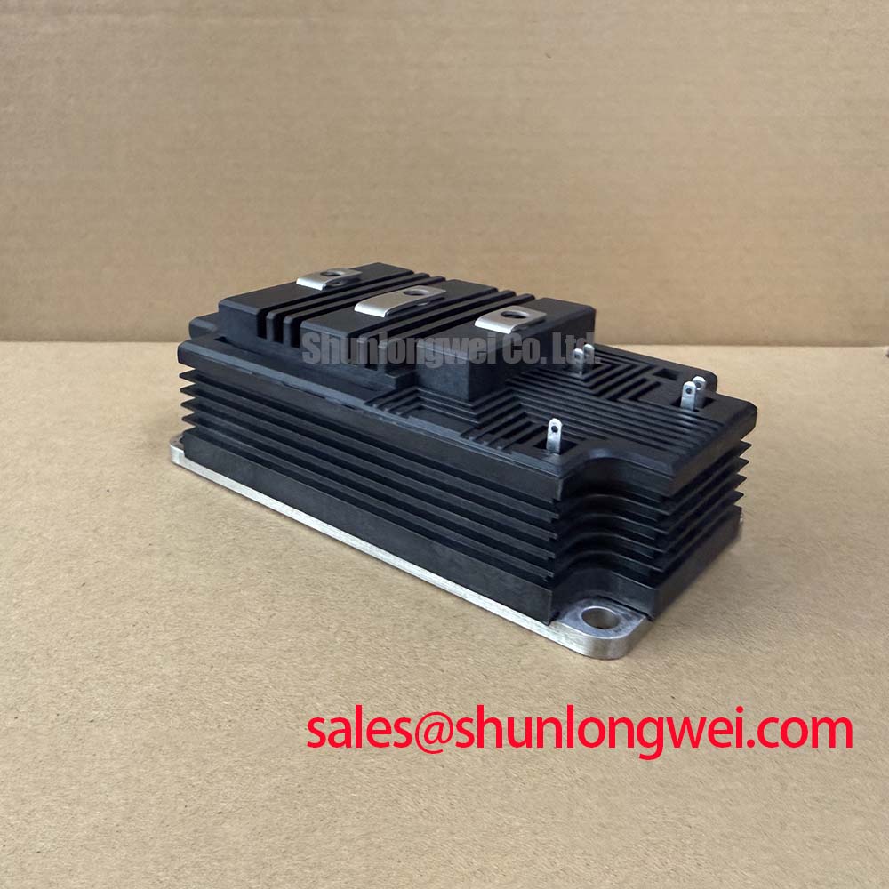
Start a service evaluation by isolating the DC link, recording the module marking, and checking the external terminals for contamination, looseness, cracking, or heat discoloration before applying any test voltage. The Hitachi MBM200H45E2-H is a high-voltage IGBT module specified for a 4500V collector-emitter voltage, 200A continuous collector current, and 10.2kVrms isolation voltage. Its H-Series style package is intended for high-voltage isolation and stable heat sinking, subject to confirmation of the original equipment mechanical interface.
| Parameter | Official Specification | Engineering Relevance |
|---|---|---|
| Collector-emitter voltage, VCES | 4500V | Applicable for evaluation in nominal 3.0kV to 3.3kV DC-link systems, with complete system verification |
| Continuous collector current, IC | 200A | Supports assessment in high-power inverter legs and bidirectional DC-DC stages |
| Isolation voltage, VISO | 10.2kVrms | Specified for one minute at 50Hz |
| Maximum junction temperature, Tj(max) | 150°C | Thermal design must account for switching loss, conduction loss, cooling, and ambient conditions |
| Package | H-Series style | Confirm mounting, clearance, terminal arrangement, and heatsink compatibility from the equipment documentation |
Transient Dynamics and Electrical Design for Active Miller Clamp Evaluation
When a replacement module is installed in a commercial string inverter or micro-grid energy-storage converter, begin by comparing the gate-drive wiring with the known-good phase leg. The control board, isolation barrier, gate return path, and power loop should be inspected as one switching system. The module rating does not define the required gate voltage, gate resistance, dead time, active Miller clamp threshold, or negative bias. Those values remain system-determined and must be verified against the original drive documentation and switching waveforms.
An active Miller clamp is an external gate-driver function used to restrain unwanted gate voltage movement during the opposite device’s high dv/dt transition. A low-impedance clamp path can reduce the possibility of parasitic turn-on, but only when the driver location, emitter return, isolation barrier, and power-loop inductance are controlled together. If the design uses a negative off-state gate bias, the proposed bias range must be validated against the gate-emitter limits stated in the applicable Hitachi documentation rather than assumed from another IGBT family.
For bench troubleshooting, use an isolated differential probe and observe gate-emitter voltage, collector-emitter voltage, and phase current during a controlled low-energy test. Ringing on the gate waveform may indicate excessive loop inductance, an unsuitable damping network, probe-ground error, or an impedance mismatch in the driver path. Check the signal at the driver output and again at the module terminals. Industrial isolation amplifiers or digital isolators should also be reviewed for common-mode transient immunity because a high-voltage switching edge can disturb the control signal without producing an obvious static fault.
Keep the gate loop physically separate from the collector switching path, minimize its enclosed area, and route the gate return directly to the driver reference. Clearance and creepage around high-potential terminals must be established from the complete insulation system, pollution environment, working voltage, and applicable equipment standard. The IGBT Design & Integration resource provides broader guidance for coordinating gate drive, thermal management, and converter topology.
Assembly Integrity and Thermal Interface Control
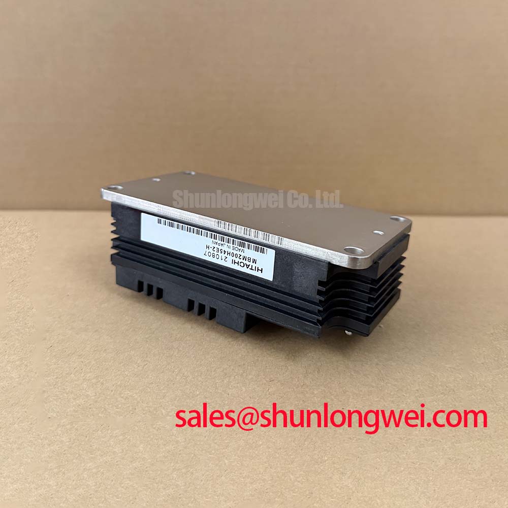
After electrical screening, inspect the heatsink surface and module base interface. The H-Series style package requires a mechanically stable heat path; the correct mounting pattern, screw sequence, and torque must come from the equipment or module assembly documentation. Thermal interface material should be applied as a uniform, controlled layer without trapped contamination or visible voids. The exact material and thickness are system assembly decisions, not official MBM200H45E2-H electrical ratings.
Baseplate flatness, heatsink distortion, uneven fastener loading, and repeated thermal cycling can alter contact pressure across the mounting surface. Use a cross-pattern tightening method appropriate to the hardware, then inspect for movement after the assembly has settled according to the service procedure. Do not compensate for a damaged or visibly uneven heatsink with additional paste. That approach can increase thermal resistance and contaminate insulation surfaces.
⚠️ Field Alert: Disconnect the DC link and allow the equipment discharge procedure to complete before touching terminals, and follow the specified fastener torque rather than applying a generic value.
The official maximum junction temperature is 150°C. Keeping continuous operation at or below 125°C is an engineering recommendation supplied for field design guidance, not a separate factory rating. Actual thermal margin depends on current waveform, switching frequency, cooling airflow, heatsink performance, thermal interface condition, and enclosure temperature. Designers evaluating operation from low-kilohertz to higher-frequency switching should measure case temperature and calculate losses for the real duty cycle instead of applying a fixed frequency derating rule.
For bidirectional battery charging and discharging, review thermal cycling in both power-flow directions. The module current rating alone does not predict junction temperature or service life. Log temperature, current, switching behavior, and cooling conditions during representative charge and discharge transitions. A MOV or other surge-absorption network may be coordinated with the DC-link protection architecture, but its clamping level, energy rating, placement, and coordination with fuses or semiconductor protection must be selected from measured transient conditions.
Short-Circuit Response and Hard-Switching Transient Control
Short-circuit protection must be treated as a coordinated function of the gate driver, current sensing, desaturation or equivalent detection method, isolation channel, and control firmware. The requested detection interval and two-stage soft turn-off behavior are design targets for the surrounding converter, not confirmed MBM200H45E2-H factory specifications. Engineers should verify the module’s applicable short-circuit safe operating information and test the complete protection chain under controlled laboratory conditions.
A fast protection circuit can still create excessive collector-emitter overshoot if the turn-off path is abrupt or the commutation loop is poorly arranged. A staged response may first limit gate-drive energy and then complete turn-off at a controlled rate, but the timing and gate-current profile must be tuned from measured current and voltage waveforms. Minimize stray inductance in the high-current loop, place the snubber or clamp network according to the topology, and verify peak voltage against the 4500V VCES rating during switching tests.
During a field failure investigation, compare the gate waveform, protection flag, current sensor output, and DC-link transient capture. A missing fault record can arise from isolation upset, sensor saturation, auxiliary supply interruption, or control timing, so it should not be assigned to the IGBT without waveform evidence. Check the driver dead time and interlock operation across temperature and load conditions. The system designer determines the appropriate dead-time margin after accounting for propagation delay, device turn-off behavior, and driver variation.
In a converter with a rectifier or auxiliary power stage, topology coordination matters. The H2G150ND06M1 can be reviewed as a neutral reference point for a related front-end or auxiliary-stage evaluation, but voltage, current, thermal, and control compatibility must be established from each device’s documentation rather than assumed from package similarity.
Thermal-Electrical Optimization with Transient Thermal Impedance
For pulsed overloads, calculate junction temperature from the measured case temperature, semiconductor power loss, and the applicable junction-to-case transient thermal response. A multi-RC thermal model can represent the changing thermal impedance during a pulse, but its coefficients must come from authoritative device data or a validated thermal characterization. Do not use a generic model as proof that the 150°C maximum junction temperature will not be exceeded.
Separate conduction loss from switching loss using the actual current and voltage waveforms. In a bidirectional DC-DC stage, repeat the calculation for both current directions because duty cycle, commutation path, and cooling exposure may differ. For a string inverter, include startup, MPPT transitions, current limiting, regeneration where applicable, and fault-clearing events in the thermal review. Peak junction temperature should be checked against the worst measured case temperature and the documented thermal impedance, with the final margin determined by the system engineer.
Thermal troubleshooting is most useful when temperature measurements are synchronized with gate command and phase current. A rising case temperature with stable airflow may suggest increased loss, degraded interface contact, or a changed switching waveform; each possibility requires confirmation through measurement. Inspect airflow paths, fan control, heatsink contact, terminal torque, and DC-link ripple before replacing the module again.
When the replacement decision involves another Hitachi high-power device, engineers may place MBM200JS12EW beside this unit for a neutral documentation review. It should not be treated as a direct substitute until voltage class, current behavior, gate-drive requirements, package geometry, isolation performance, and protection data are confirmed. Converter compliance work should also be mapped to the relevant IEC 60146 Semiconductor Converters Standard. Where soft-switching is part of the topology, the operating assumptions can be compared with the principles described for ZVS resonant converters, while the actual switching behavior remains subject to measurement in the finished system.