Content last revised on October 26, 2026
MG30G2YL1 Inverter Evaluation
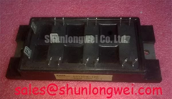
With the DC link isolated, check the inverter’s gate-to-emitter return path for unintended coupling before applying a switching command, then confirm the device identity and electrical boundary of MG30G2YL1: Toshiba module, 1200.0 V rated voltage, and 30.0 A rated current. These are official product specifications for the listed device, not calculated operating limits.
For a compact industrial inverter or high-speed CNC spindle drive, the module should be assessed as part of the complete commutation loop. Gate-driver behavior, DC-link construction, motor-cable length, cooling, protection coordination, and switching frequency all affect the final operating envelope. The external package is identified as a Toshiba Module; terminal geometry, gate-drive requirements, thermal impedance, and switching characteristics should be matched to the original equipment documentation before replacement.
Assembly Integrity and Layout Architecture for Differential Gate Emitter Loop Routing
Separate the auxiliary gate-reference return from the main high-current emitter path so that load-current voltage drops do not appear directly in the gate-drive signal. In an IGBT installation, the practical equivalent of a differential gate-source loop is a tightly coupled gate-to-emitter driver loop, routed with its intended reference conductor and kept away from the collector power path.
When inspecting a failed compact inverter, trace the driver output from the isolated driver or gate resistor to the module terminal and back through the dedicated return. Look for shared copper between the gate return and the high-current emitter connection, long unpaired conductors, connector pin changes, and routing beside switching nodes. These conditions can introduce common-emitter inductance and cause ringing, delayed turn-off, or an apparent gate-voltage disturbance during high-current transitions.
A sound layout keeps the gate loop physically compact, maintains consistent separation from collector and DC-link conductors, and avoids unnecessary vias or narrow necks in the return path. The power loop should remain symmetrical between complementary switching positions where the topology permits it. This is a design consideration rather than an MG30G2YL1 factory specification. The system designer should verify gate amplitude, turn-on and turn-off behavior, and peak transient voltage with an appropriately referenced differential probe.
Gate resistance should be selected from the driver capability, switching waveform, thermal target, and measured oscillation response. A resistor that is appropriate on a short laboratory connection may behave differently after the module is installed in a production cabinet. Miller coupling can also transfer a collector-voltage transition into the gate loop, so the driver supply decoupling and gate-return geometry need to be evaluated together.
🔧 Bench Diagnostic: Do not connect or disconnect the module gate cable while the DC link or driver supply is energized.
Suppressing DC-Link Voltage Doubling and Motor-Cable Reflections
Long motor leads can behave as a transmission-line section rather than a simple resistive load. Reflections caused by impedance discontinuity may increase the voltage appearing at the motor terminals and return stress to the inverter switching devices. The 1200.0 V rating of MG30G2YL1 is an official device rating; it does not define the permissible overshoot of a particular drive installation.
Begin the investigation at the inverter output, then compare the waveform at the motor terminals with the cable disconnected or replaced by the approved test arrangement. A large difference between the two locations points the investigation toward cable impedance, termination, common-mode paths, or output-filter interaction. The oscilloscope setup must have suitable bandwidth, probe insulation, and common-mode rejection for the switching environment.
Output chokes, dv/dt filters, or sine-wave filters may be considered when the installed motor cable and motor insulation system require additional transition control. Their selection is system-dependent and should account for motor current, carrier frequency, filter resonance, grounding, bypass behavior, and thermal loading. Do not treat a generic filter value as a guaranteed accessory specification for this Toshiba module.
Freewheeling diode recovery can also influence the commutation event. A fast reverse-recovery current can combine with stray inductance to create voltage overshoot and radiated electromagnetic interference. Snubber networks, local DC-link decoupling, and carefully arranged bus connections can reduce the energy associated with the transition, but the component values must be established from measured switching waveforms and loss calculations.
| Device | Manufacturer | Official rated voltage | Official rated current | Engineering use |
|---|---|---|---|---|
| MG30G2YL1 | Toshiba | 1200.0 V | 30.0 A | Compact inverter and spindle-drive evaluation |
| MG400V2YS60A | Toshiba listing reference | Verify from its applicable datasheet | Verify from its applicable datasheet | Neutral same-family comparison reference |
The comparison reference is not a substitute recommendation. Mechanical fit, terminal arrangement, gate characteristics, thermal interface, and protection coordination must be checked independently. Engineers reviewing the wider power stage may also examine the MG200Q2YS1 as a neutral reference for an upstream or auxiliary stage, subject to the actual circuit topology.
The relationship between switching transitions, parasitic inductance, and output filtering is also relevant to buck converter power-topology behavior. Semiconductor manufacturers’ application material, including the STMicroelectronics IGBT and power transistor resources, provides useful general context, but it does not replace Toshiba-specific operating data.
Field Diagnostics for Cres-Induced Gate Voltage Spikes
High collector-voltage slew rates can couple through device capacitances and raise the inactive IGBT gate voltage. In a half-bridge, that disturbance may reduce the effective dead-time margin and create a risk of cross-conduction. The correct response is to examine the complete gate waveform at the module terminals, not only the driver output at the control board.
Use a short, controlled measurement connection and observe both the commanded gate signal and the gate-to-emitter voltage during the opposite switch transition. Compare the waveform with the power stage disabled, at reduced test energy where appropriate, and under the intended switching condition. A gate spike that appears only after the power loop is connected may indicate coupling through layout, common-emitter inductance, driver isolation capacitance, or probe reference error.
An active Miller clamp can provide a low-impedance holding path during the off-state transition when the selected driver supports that function. A negative gate bias may also be evaluated as a design consideration, including the requested range of −5 V to −15 V, but this must not be treated as an MG30G2YL1 factory requirement. The driver, insulation system, gate-emitter limits, startup sequence, and fault behavior must all be validated before such a bias is applied.
Keep the clamp path and gate-return path physically close to the module terminals. Separate isolated driver supplies for complementary positions can help prevent supply-current coupling, while local decoupling should be placed according to the driver manufacturer’s layout guidance. If the measured gate spike changes significantly when the probe connection is moved, correct the measurement method before changing the circuit.
For a replacement in a CNC spindle drive, verify the original gate-driver topology, dead-time, desaturation or overcurrent protection, motor-cable arrangement, and cooling interface. The Field Engineer’s Handbook can be used as a supporting reference for structured testing, failure analysis, and reliability review without assigning unverified FIT, SEB, cosmic-ray, altitude, or service-life figures to this product.
Commissioning Checks for Thermal and Power-Stage Coordination
Before energizing the complete inverter, confirm that the replacement module’s 1200.0 V voltage class and 30.0 A current rating correspond to the equipment’s documented electrical conditions. The current rating alone does not establish allowable current under every switching, cooling, duty-cycle, or ambient condition.
Inspect the thermal interface for even contact, clean mounting surfaces, and a correctly controlled interface material. Confirm that the heatsink, airflow, temperature sensing, and fault shutdown remain functional after installation. A module that passes a static resistance check can still exhibit switching or thermal problems, so commissioning should progress from low-energy gate checks to controlled power-stage operation while recording collector-emitter voltage, gate-emitter voltage, current, and heatsink temperature.
For battery-fed bidirectional DC-DC equipment, repeated charge and discharge transitions can impose thermal cycling on the complete power assembly. The system designer should review semiconductor losses, busbar flexibility, cooler response, capacitor ripple current, and protection timing as a combined reliability problem. No specific lifetime or cycle count should be assigned to MG30G2YL1 without a defined mission profile and supporting test data.
Where a thyristor trigger stage shares the cabinet, its trigger current, trigger voltage, pulse width, and pulse-train behavior should be checked independently from the IGBT gate circuit. A strong trigger pulse does not correct an incorrectly referenced IGBT gate drive, and auxiliary boost-capacitor charging paths should be evaluated for high-frequency diode recovery and supply-current interaction.