Content last revised on October 10, 2026
MG50G6ES40 Replacement Evaluation
- Isolate the DC link and confirm the discharge condition before touching the power stage.
- Check the cold-state impedance between the main power terminals and gate control terminals against a known-good unit.
- Inspect terminal surfaces, mounting flatness, insulation barriers, and heatsink contact for mechanical damage.
- Confirm that the gate driver supply, isolation, interlock, and feedback wiring match the original motion-control design.
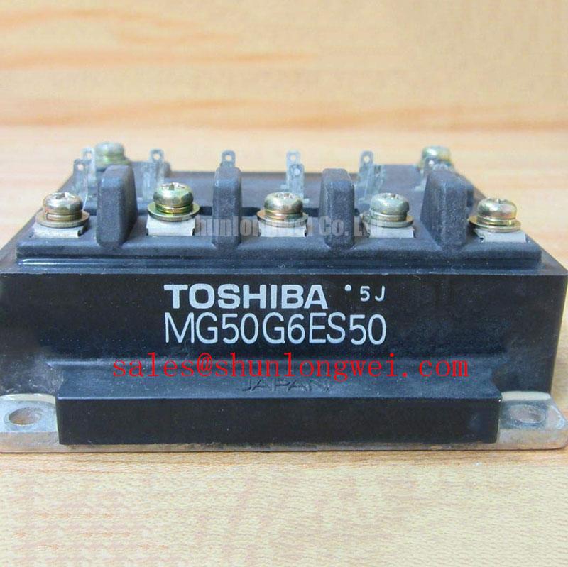
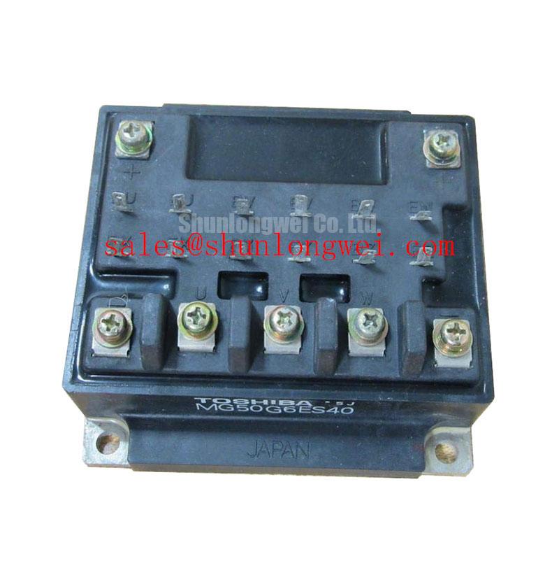
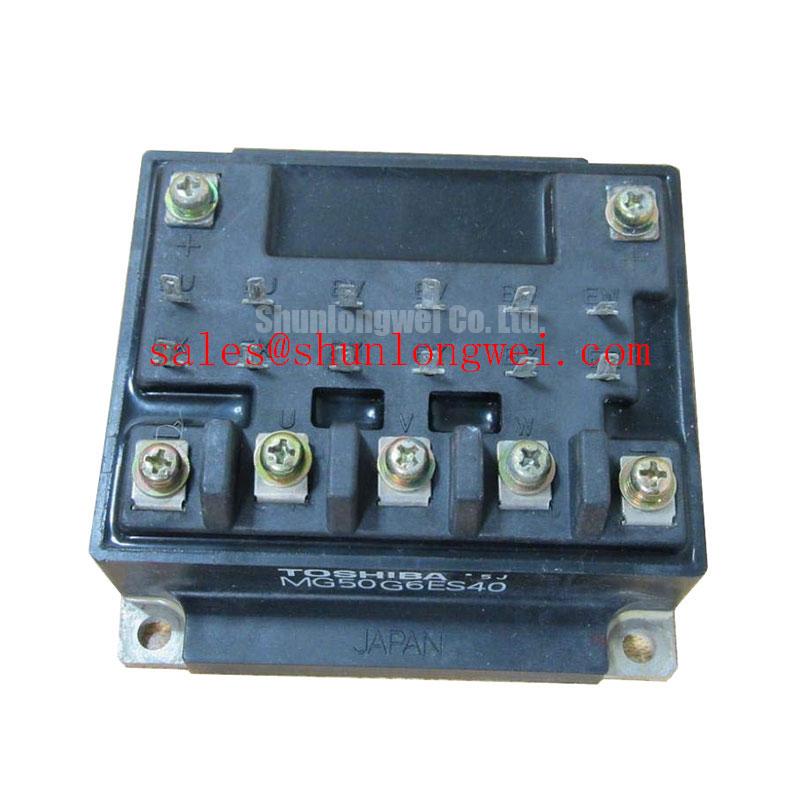
The Toshiba MG50G6ES40 is identified for replacement evaluation as a 600.0 V, 50.0 A IGBT Module in a Toshiba Module package. These are official specification values supplied for this product page. The rating does not by itself define the allowable switching frequency, short-circuit duration, braking duty, or thermal operating point, so the service decision should begin with the original servo inverter topology and its measured electrical stresses.
| Manufacturer | Toshiba |
| Part number | MG50G6ES40 |
| Rated voltage | 600.0 V, Official Specification |
| Rated current | 50.0 A, Official Specification |
| Package | Toshiba Module, Official Specification |
| Typical evaluation target | Precision stepper and BLDC motor servo motion actuators |
For a failed axis amplifier, record the gate-to-emitter and collector-to-emitter readings before removing the module. A shorted power path can also damage the gate driver, current sensor, bootstrap network, clamp components, or DC-link fuse. Replacing the power module without checking those surrounding circuits can reproduce the original failure during the first enable command.
MG50G6ES40 Circuit Protection and Reliability: Calibrating Fault-Clearing Dynamics
Short-circuit protection must be coordinated around the gate driver, current-sensing path, and the actual switching loop rather than treated as a property guaranteed by the module rating. A desaturation circuit, when present in the host inverter, detects a rapid loss of collector-emitter saturation margin and initiates gate shutdown. The designer may use a Type I response for rapid interruption or a Type II sequence that first reduces gate drive and then completes turn-off, but the selected method must be validated against the driver architecture and the module’s short-circuit safe operating area data.
For a control system targeting fault recognition within 10 µs, treat that interval as a system-level design target, not as an official MG50G6ES40 specification. Propagation delay through the desaturation diode, blanking network, isolator, driver output stage, and gate loop all contribute to the actual response. A bench test should capture the gate-emitter voltage, collector-emitter voltage, phase current, and driver fault signal on the same time base. The useful question is whether the protection sequence clears the fault before inductive energy drives the switching node beyond the verified voltage margin.
Two-stage soft turn-off can reduce the voltage spike created when stored current is interrupted abruptly. The first stage lowers gate drive current, limiting the rate of current collapse; the second stage completes isolation after the collector voltage has begun to rise. This approach requires careful coordination with the driver’s fault latch and reset logic. Excessively slow shutdown can increase short-circuit energy, while an overly aggressive response can create inductive overvoltage. The correct balance is established through controlled testing with the actual DC-link capacitor, busbar, load inductance, and gate-loop layout.
Keep the desaturation return path separate from high-current emitter or source circulation paths where the driver layout permits. Parasitic voltage in the emitter connection can corrupt the sensed gate-emitter reference and create either nuisance trips or delayed protection. If a repaired actuator reports an intermittent overcurrent event, inspect the driver reference connection, isolation supply stability, fault-clear timing, and connector contact pressure before assigning the fault to the IGBT itself.
The MG50Q1BS1 may be reviewed as a separate Toshiba family option during a cross-reference study, but electrical topology, terminal arrangement, gate characteristics, and mechanical fit must be checked independently before any substitution decision.
Preventing Spurious Faults: Mitigating Commutation Turn-Off Voltage Spikes
Commutation overshoot is often driven by the interaction between the antiparallel freewheeling diode, stray inductance, gate resistance, and the DC-link layout. During diode recovery, reverse current can rise sharply and then collapse, producing a high di/dt event that couples into the switching loop and control reference. The MG50G6ES40 page identifies the voltage and current ratings, but it does not establish a guaranteed reverse-recovery profile or a fixed snubber value for every converter layout.
Use a double-pulse or equivalent switching test to observe the diode recovery current, collector-emitter voltage, gate waveform, and local DC-link voltage at the module terminals. A “snappy” recovery signature may appear as a narrow voltage excursion and ringing burst, while excessive gate resistance can extend switching loss and raise device temperature. The practical adjustment is to evaluate turn-on gate resistance, turn-off gate resistance, driver current capability, and the physical commutation loop together. A resistor selected only from a schematic value can behave differently once connector inductance, busbar spacing, and mounting geometry are included.
An RC snubber can damp high-frequency ringing when it is placed close to the switching loop and selected from measured waveform energy. It should not be added as a universal cure without checking resistor pulse capability, capacitor voltage rating, thermal dissipation, and its effect on turn-off loss. Designers should also compare the switching waveform at the module pins with the waveform measured farther away at the DC-link capacitor; a large difference points toward layout-induced inductance rather than a simple gate-drive fault.
Fast semiconductor fuse coordination is a separate protection layer. Compare the fuse clearing I²t with the inverter’s prospective fault current, the module’s surge capability, and the mechanical energy available in the DC link. The fuse must interrupt rapidly enough to prevent destructive fault persistence, yet its pre-arcing behavior must not conflict with normal motor acceleration or regenerative events. This coordination is determined by the complete power stage, not by the 50.0 A nominal module rating alone.
Where a bootstrap driver supplies the upper switch, inspect the bootstrap capacitor charging path, diode recovery behavior, and high-frequency charge balance during repeated PWM operation. A weak bootstrap supply can produce a distorted gate waveform that resembles a semiconductor failure. The related 2MBI50J-060 can be considered as a separate power-stage reference when reviewing the wider converter topology, subject to its own electrical and mechanical verification.
⚡ Field Alert: Disconnect control power and the DC link before removing gate or power connectors, and follow the original inverter’s discharge and interlock procedure.
Transient Dynamics and Electrical Design: Thermal Cycling Margins for Braking Operation
Braking design begins with the motor’s deceleration profile and the energy transferred into the DC link. The braking path may use an external braking IGBT and ballast resistor, while some assemblies use a topology-specific integrated arrangement; the available product data for MG50G6ES40 does not establish an internal braking circuit, so the service engineer should identify the actual schematic before assuming one.
Measure the DC-link rise during the fastest permitted deceleration, then correlate that waveform with braking-command timing, resistor temperature, and the switching waveform at the braking transistor. The resistor must absorb the required pulse energy without exceeding its pulse, thermal, and insulation limits. The braking switch must also remain within its voltage, current, switching-loss, and junction-temperature boundaries. A 600.0 V rating is an official product parameter, not a permission to operate the DC link continuously at that level during regenerative transients.
Thermal cycling is governed by the difference between junction temperature and case temperature, the duration of each braking event, mounting flatness, thermal interface quality, and the cooling system response. Repeated short braking pulses can produce a different stress pattern from one long deceleration. Check the heatsink contact after service, remove old interface material without damaging the mounting surface, and apply the replacement interface according to the equipment manufacturer’s assembly practice. Clamping uniformity matters because local contact variation can increase thermal resistance and accelerate temperature excursions.
Positive temperature coefficient behavior can assist static current sharing when multiple parallel devices are deliberately designed into a stage, but dynamic sharing still depends on matched gate loops, common-emitter inductance, propagation delay, and symmetrical busbar geometry. Do not assume that parallel connection is acceptable simply because the nominal current is 50.0 A. The system designer must verify current distribution during turn-on, turn-off, short-circuit response, and regenerative braking.
For servo systems using precision stepper or BLDC actuators, examine the relationship between commanded deceleration, position-loop response, and DC-link protection. A control-loop fault can repeatedly trigger braking pulses even when the power module is healthy. Review encoder feedback, drive enable timing, overvoltage thresholds, and braking resistor temperature together. If gate pulses appear correct but the DC link rises abnormally, investigate regenerative energy flow and braking control before replacing the module again.
Thermal packaging studies may also reference Thermal Shock Testing for Power Modules when evaluating repeated temperature transitions, while broader semiconductor test terminology can be checked through the JEDEC Global Standards resource. These references do not constitute a product-specific lifetime guarantee. For switching-loop layout and device-level reliability context, the engineering discussion Unlocking Efficiency in Industrial Drives provides additional background, while final acceptance remains dependent on measured waveforms, cooling conditions, and the original equipment limits.