

Content last revised on October 30, 2026
Field Diagnostics & Commissioning: Insulation Barrier Integrity in MUBW50-12E8 Topologies
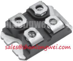
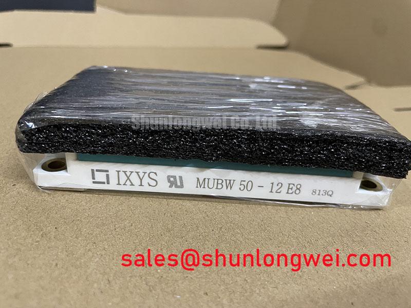
With the DC link discharged and the power stage isolated, compare the rectifier, inverter, and brake-chopper paths against the equipment schematic before reconnecting the gate-driver board. For the IXYS MUBW50-12E8, these functions belong to the same PIM (Power Integrated Module), so a fault investigation should distinguish the affected circuit rather than treat every abnormal reading as an inverter failure.
The specified ratings include an input-rectifier repetitive reverse voltage, Vrrm, of 1600 V; an inverter collector-emitter voltage, Vces, of 1200 V over Tvj = 25°C to 150°C; a dedicated brake-chopper Ic80 rating of 35 A at a case temperature of 80°C; and a module isolation test voltage, Visol, of 2500 V AC RMS for 1 minute. The brake-chopper current is not an inverter-current rating, and the isolation test voltage is not a continuous operating-voltage allowance.
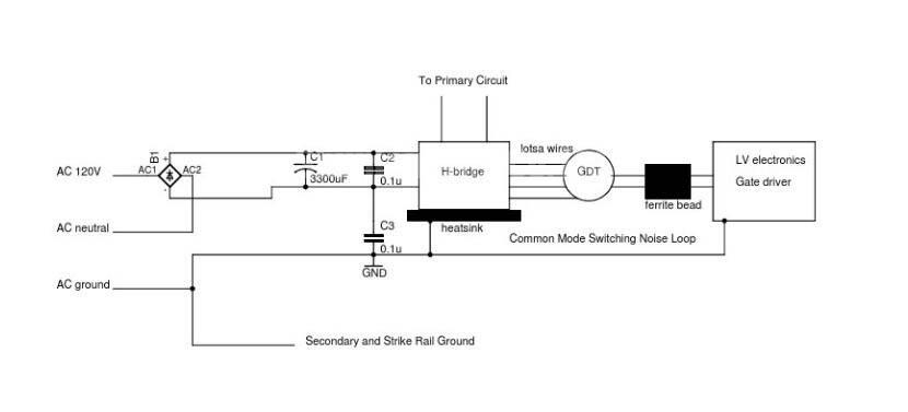
Trace the isolation boundary between the power terminals, mounting interface, gate-driver supplies, and control electronics before selecting an insulation test procedure. The module’s stated isolation test does not, by itself, establish reinforced insulation for the completed equipment. That classification depends on the complete barrier construction, working voltage, creepage, clearance, and applicable equipment requirements. Likewise, common-mode transient immunity belongs to the selected driver and its implementation; it is not established by the module’s Visol rating.
Design Consideration: Inspect contamination paths and damaged insulating hardware around the mounting area without assuming that a clean exterior proves dielectric integrity. Disconnect sensitive electronics as required by the equipment service procedure before any insulation test. Test connections and acceptance criteria should follow the applicable manufacturer instructions, because a test intended for a disconnected power module can overstress attached driver circuitry.
For nuisance trips during switching, examine the isolated driver supply and gate-emitter waveform together. A disturbance appearing at the controller interface can originate from common-mode coupling, an unstable local supply, or measurement pickup. Use probes with suitable isolation and common-mode performance, and minimize their connection loops. Comparing the affected channel with another channel under equivalent conditions helps distinguish a circuit problem from an instrumentation artifact.
In a compatibility assessment for a heavy-duty variable-frequency AC motor drive, the rectifier feeds the DC link, the inverter controls the motor phases, and the brake chopper provides a controlled path to an external braking resistor. During regeneration, that resistor must absorb energy according to the equipment’s stopping duty and thermal design. The 35 A chopper rating alone does not specify permissible braking energy, resistor resistance, or repetitive stopping capability.
A separate power stage built around a module such as CM200DU-24H is a different architectural case, not an assumed companion connection. Engineers comparing these arrangements should map the rectification, switching, and braking functions explicitly before assessing shared DC-link hardware or protection interfaces.
Preventing Spurious Faults: Thermal Paste Degradation Prevention and Mounting Guidelines for MUBW50-12E8
Inspect the heatsink contact surface for residue, raised damage, and uneven seating before applying fresh thermal interface material. A disturbed interface can change the temperature distribution without producing an obvious electrical fault during a cold check. Record the condition of the removed interface and compare it with the mounting footprint rather than judging thermal contact from the quantity of paste remaining at the edges.
Design Consideration: Select the interface material and application method around the specified mating surfaces, flatness, mounting arrangement, and operating temperature. The objective is continuous contact with limited voiding, not a thick layer intended to compensate for mechanical distortion. Final bond-line thickness and fastening torque belong to the approved assembly specification; they should not be borrowed from another module merely because its outline appears similar.
Bring the module into contact evenly using the documented fastening sequence. Check that terminal connections do not pull the package away from the heatsink or impose bending loads after mounting. If the contact pattern remains uneven, investigate the heatsink surface and mechanical stack instead of increasing screw torque. Belleville-spring pressure calibration, press-pack clamping, and double-sided cooling procedures are not interchangeable with the mounting instructions for this module and should not be introduced without supporting mechanical documentation.
After reassembly, compare temperatures at consistent locations under repeatable load conditions. A local rise can reflect interface resistance, airflow distribution, electrical loss, or sensor placement. Correlating temperature behavior with current and switching activity is more useful than assigning a single cause from a thermal image. Where the equipment permits inspection after testing, movement or separation of the interface material can help explain changes between successive thermal runs.
Parallel operation requires separate electrical validation. A favorable temperature coefficient of collector-emitter saturation voltage can assist static current sharing only within the relevant operating region; it does not establish balanced dynamic current for the MUBW50-12E8. Branch resistance, gate-loop impedance, propagation delay, and thermal coupling remain important. Symmetrical current paths should therefore be assessed together with branch-current measurements rather than treated as sufficient proof of sharing.
The Arrhenius equation explains a temperature-dependent reaction-rate relationship, but it does not supply a module lifetime without a validated degradation model. Similarly, the Peltier effect describes thermoelectric heat transfer, not a cooling feature specified for this product. Neither concept replaces measurement of the actual mounting interface and heatsink performance.
Assembly Integrity & Layout Architecture: Mitigating Hard-Switching Transients for MUBW50-12E8
Measure collector-emitter overshoot at the switching device with a probing arrangement that does not add a large pickup loop. Turn-off voltage reflects the interaction between current slew rate and stray inductance, so a satisfactory DC-link reading does not establish the transient stress at the module terminals. Capture the gate command, gate-emitter voltage, and power-stage response together to identify whether a disturbance begins in the driver or the commutation path.
Design Consideration: Reduce the enclosed area of the high-current commutation loop while keeping the gate-drive return distinct from power-current paths wherever the terminal arrangement permits. Mechanical accessibility should not force long, separated DC-link connections. Clearance and creepage must still satisfy the equipment’s insulation requirements; compact layout is not a reason to narrow an electrical barrier.
Pro Tip: Keep the DC-link current paths geometrically balanced where the topology permits, then verify turn-off overshoot and current distribution with controlled double-pulse measurements.
Short-circuit protection should account for both turn-on into an existing fault and a fault developing during conduction. Detection blanking, sensing delay, driver propagation, and shutdown behavior all contribute to the stress interval. A generic microsecond response target is not an established short-circuit withstand rating for this module. Protection timing must instead be coordinated with the manufacturer’s applicable safe-operating-area limits and the actual fault conditions.
A staged soft turn-off can reduce the abruptness of fault-current interruption, but slower shutdown also changes the energy dissipated in the switching device. Designers should evaluate that trade-off using the selected driver, bus voltage, fault impedance, and temperature conditions. Check whether a protection event latches the affected channel, disables complementary switching, and prevents automatic restart into a persistent fault.
Regenerative braking deserves its own protection review because it can raise DC-link voltage while the inverter is otherwise operating normally. Check the chopper command path, resistor continuity, temperature protection, and DC-link sensing against the equipment schematic. An overvoltage event can involve the resistor circuit, control timing, incoming supply conditions, or the braking duty; the fault message alone does not identify a failed chopper.
For cross-model sourcing, FP30R06W1E3_B11 is a comparison reference rather than a declared substitute. Consult the respective datasheets for voltage class, current conditions, internal circuit, terminal mapping, thermal characteristics, and mounting details before considering interchangeability. A package resemblance or a matching equipment description cannot establish electrical compatibility.
Assembly Integrity & Layout Architecture: Active Miller Clamp Implementation for MUBW50-12E8
Observe the off-state gate-emitter waveform while the complementary switch commutates to assess unwanted gate movement. Collector-voltage transitions couple displacement current through gate-collector capacitance; impedance in the gate discharge path can convert that current into a gate-voltage excursion. Measurement should distinguish genuine terminal voltage from probe-loop pickup before changes are made to the driver.
Design Consideration: An active Miller clamp can provide a low-impedance discharge path when the gate is commanded off. Its effectiveness depends on placement, connection inductance, activation behavior, and compatibility with the driver output stage. Route the clamp close to the relevant gate and emitter connections, following the actual terminal definition rather than assuming a separate Kelvin-emitter connection exists.
Negative gate bias is a system-level option, not a prescribed setting for the MUBW50-12E8. Its suitability depends on the permitted gate-emitter limits, driver supply behavior, and measured transients. Evaluate both normal switching and fault shutdown, since supply ringing or emitter movement can increase the voltage stress seen at the gate terminals. Clamp action and supply bias should be assessed as interacting functions rather than independent fixes.
Dead time also requires waveform-based adjustment. Too little separation can permit simultaneous conduction, while excessive separation can change diode conduction and switching behavior. Compare the actual turn-off completion of one device with the complementary device’s turn-on across relevant current, temperature, and driver-supply conditions. Controller command timing alone does not include all propagation and switching delays.
The Wide Bandgap Revolution technical overview provides broader context for switching-speed and gate-loop challenges in SiC and GaN systems; those device-specific limits should not be transferred to this IXYS IGBT module. For the repaired assembly, finish validation by recording off-state gate excursions, complementary switching timing, and driver behavior during controlled shutdown, then compare those measurements with the approved circuit requirements.