
Content last revised on September 27, 2026
P546A2007 Circuit Protection and Reliability: Calibrating Turn Off di/dt Induced Vpeak Clamping
| Parameter | Specification |
|---|---|
| Manufacturer | Vincotech |
| Model | P546A2007 |
| Product Category | IGBT Module |
| Blocking Voltage, VCES | 600 V |
| Collector Current Rating, IC | 30 A; refer to the manufacturer’s datasheet for rating conditions |
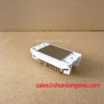
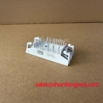
| Module Configuration | PIM: three phase rectifier, inverter and brake chopper |
| Silicon Technology | Trench Fieldstop IGBT |
| Isolation Voltage | 2500 V; refer to the manufacturer’s datasheet for test conditions |
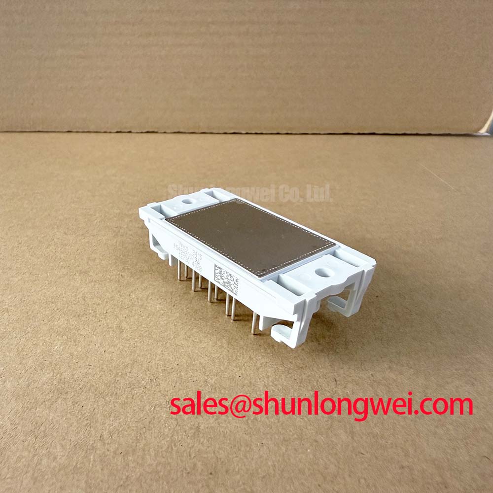
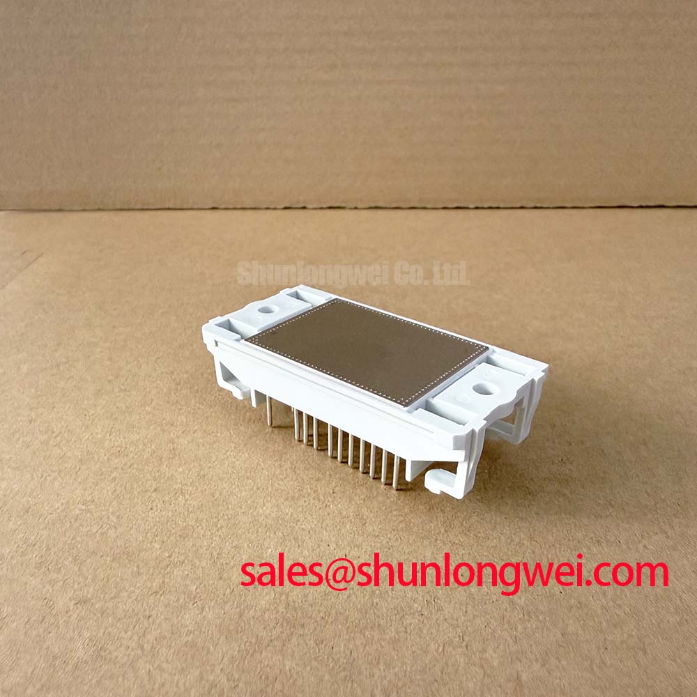
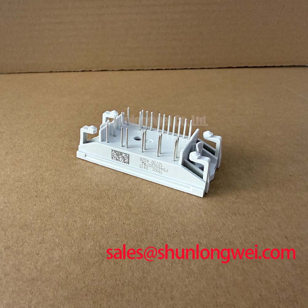
| Package and Housing | flow 0 Clip in |
Measure the switch node with a properly rated differential probe while comparing the turn off overshoot against the actual DC link voltage and the 600 V VCES blocking rating; a clipped or repeated overshoot pattern requires the commutation loop, clamp network and gate timing to be checked together.
The relevant engineering relationship is that the transient peak rises with the DC bus voltage, stray inductance and the rate of current fall. This makes the complete power loop more important than the module rating alone. The P546A2007 integrates a three phase rectifier, inverter and brake chopper in a PIM configuration, so the rectifier path, inverter switching loop and braking path should be traced separately during a service investigation.
Design Consideration: Keep the high current commutation path short, symmetrical and physically close to the module terminals. A planar busbar arrangement can reduce unequal current sharing and parasitic inductance, but the acceptable residual inductance must be established by switching waveform measurements on the finished assembly rather than assumed from a mechanical drawing. Snubber capacitors, MOVs and DC link capacitors should be evaluated as a coordinated overvoltage network. The system designer should select their voltage, energy and pulse capability from the measured transient waveform and fault conditions.
At the bench, inspect the busbar joints, clamp terminals, cracked insulation, loose fasteners and signs of localized heating before energizing the inverter. With power removed and the DC link safely discharged, compare cold resistance readings between corresponding phase paths and brake chopper terminals against a known good assembly. A low resistance reading can reflect a damaged semiconductor, a parallel circuit path or connected protection hardware, so isolate the surrounding network before assigning a fault to the module.
Clearance and creepage around the high voltage terminals must be maintained according to the equipment insulation design, contamination level and applicable safety standard. The listed 2500 V isolation voltage is a module test specification, not a continuous working voltage rating or an automatic certification of the finished forklift controller. Engineers evaluating broader semiconductor standards and test terminology can consult the JEDEC Global Standards for the Microelectronics Industry.
For the upstream or complementary power path, the FS15R06VE3_B2 may be reviewed as a separate topology component. Its electrical role, switching behavior and thermal path must be assessed independently rather than inferred from the P546A2007 specification.
P546A2007 Thermal Electrical Optimization: Negative Gate Bias and Active Miller Clamp Tuning
Probe the gate emitter waveform directly at the module terminals during the suspected false turn on event, then compare it with the opposite switch command and the emitter reference at the driver output; this separates gate loop ringing, common mode movement and driver timing faults that may otherwise appear as unexplained shoot through.
The P546A2007 is specified as a Trench Fieldstop IGBT module, but the supplied hardware data does not define a gate voltage range, gate charge, switching speed, gate resistor value or negative turn off bias. Those values must therefore come from the applicable Vincotech technical documentation and the actual gate driver design. Do not apply a negative gate voltage or a fixed resistor value solely because it is common in another IGBT platform.
Design Consideration: A dedicated active Miller clamp can provide a low impedance path that holds the inactive gate near its intended turn off state during a high dv/dt transition. Its effectiveness depends on the driver reference, gate loop inductance, clamp threshold, source and sink capability and the physical distance between driver and module. The system engineer should verify the resulting gate emitter waveform at the module pins, not only at the driver board.
Gate resistor selection is an engineering tuning task. A smaller resistance can increase switching speed and voltage overshoot, while a larger resistance can reduce ringing at the cost of switching loss. The practical starting point should be selected from the driver current capability and the switching loss budget, then adjusted using double pulse or representative inverter tests. Any gate damping change should be checked for both turn on and turn off behavior because the two transitions can have different parasitic paths.
Common mode ground bounce deserves particular attention in a PIM assembly. Route the gate return with the intended emitter reference, avoid sharing it with high current power returns, and examine the driver supply during the same capture. A shield or guard strategy can help in a noisy traction controller, but its connection must not create a new circulating current path. The P546A2007 data supplied here does not identify a Kelvin emitter terminal, so the integrator should use only the terminals defined in the original module documentation.
When reviewing alternative hardware, the CM30TF-12E can be evaluated as a separate replacement candidate only after confirming topology, terminal assignment, voltage, current, isolation, housing and gate drive compatibility. Mechanical fit alone is not evidence of electrical interchangeability.
P546A2007 Operational Boundaries: Evaluating Junction to Case Thermal Network Simulation Limits
Use a thermocouple or suitable case temperature method at the defined mounting interface while recording phase current, switching frequency, duty cycle and ambient conditions; compare the measured thermal trend with the controller’s loss estimate before treating an overtemperature trip as a semiconductor failure.
The listed collector current rating is 30 A under the manufacturer’s specified conditions, but current capability in service is not determined by that number alone. Conduction loss, switching loss, duty cycle, cooling method, interface quality, ambient temperature and neighboring heat sources all influence junction temperature. A short overload pulse may produce a different thermal response from a sustained traction load, so the simulation should represent the actual current waveform instead of using only an average value.
Engineering Recommendation: A junction to case thermal model may use multiple RC sections to represent transient heating, but every resistance and time constant must come from the relevant manufacturer thermal data or a validated measurement method. The model output should be checked against case temperature and switching loss measurements. Without those inputs, a simulated peak junction temperature is only an estimate and should not be presented as a guaranteed operating limit.
Inspect the mounting surface for contamination, distortion and uneven contact. The flow 0 Clip in housing requires the mechanical retention method to be compatible with the equipment assembly and the manufacturer’s installation instructions. Thermal interface material should cover the intended contact area consistently without contaminating insulation surfaces. Parallel heat paths, pressure distribution and the condition of the heatsink should be checked when a replacement module runs hotter than the removed unit.
Electrical and thermal faults can overlap. A partially damaged IGBT may show acceptable cold resistance yet produce abnormal switching loss under load; a poor thermal interface can produce a similar field symptom without an electrical short. Capture collector emitter voltage, gate emitter voltage and phase current together where the test setup permits, and compare the result with a known good waveform. Do not infer lifetime, failure rate or overload endurance from the nominal 30 A value.
Preventing Spurious Faults: DC Bus Operating Voltage Headroom for P546A2007
Record the actual DC bus voltage at the module terminals during acceleration, regenerative braking and emergency stopping, then correlate each protection trip with the measured bus waveform, brake chopper command and inverter switching state.
The P546A2007 has an official blocking voltage rating of 600 V. That value defines an important device boundary, but it does not prescribe a universal DC bus setting or a fixed derating percentage for every traction controller. Bus ripple, regenerative energy, wiring inductance, braking response, temperature and protection reaction time must be evaluated as a complete system.
Design Consideration: Establish voltage headroom by measuring the highest credible transient at the module terminals and validating the clamp and brake chopper response under the most demanding operating condition. The DC bus capacitor bank, MOV network, braking resistor and control firmware should be reviewed together. A protection circuit that works during a slow regenerative event may respond differently during a rapid contactor transition or an inverter fault.
Altitude, terrestrial radiation and single event burnout require application specific reliability data. No FIT rate, neutron flux limit, SEB probability or altitude derating value is established by the supplied P546A2007 parameters, so those figures should not be assigned to this module without a qualified manufacturer source or an appropriate reliability study. The same rule applies to service life and safety certification claims.
For practical troubleshooting, inspect the DC link precharge circuit, braking resistor connections, contactor timing and voltage sensor calibration before replacing the power module. Verify the oscilloscope probe rating, differential input connection and discharge procedure. ⚠️ Field Alert: Disconnect the power source and confirm the DC link is discharged before removing module terminals or connecting a measurement probe.
During a replacement assessment, verify the PIM topology, terminal layout, isolation requirement, cooling arrangement and gate driver behavior as one compatibility set. The Wide Bandgap Revolution reference can support broader switching technology comparisons, but it does not change the silicon IGBT specifications of the P546A2007.