Content last revised on September 16, 2026
PM150RL1B060 Product Overview and Benchtop Waveform Tuning
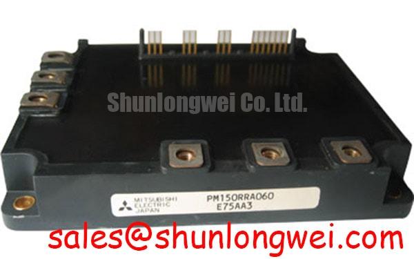
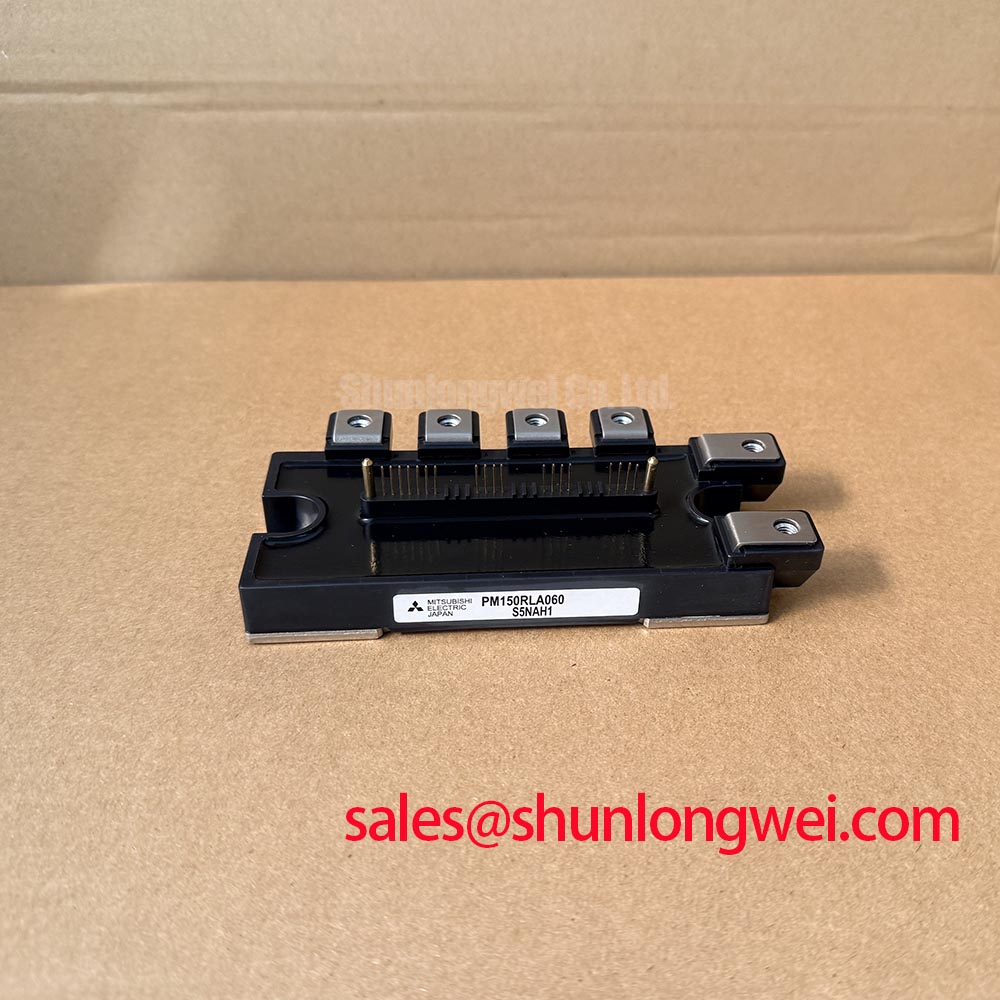
With the DC bus fully isolated, inspect the module body for cracks, carbon tracking, loose terminals, or distorted mounting surfaces before checking terminal-to-terminal cold resistance against a known-good reference. The PM150RL1B060 is a Mitsubishi Electric IPM specified at 600 V collector-emitter voltage and 150 A collector current at Tc = 25°C. Its seven-pack configuration combines inverter and brake functions for industrial motor-drive power stages.
| Parameter | Official Specification | Engineering Significance |
|---|---|---|
| Manufacturer | Mitsubishi Electric | Confirm the original equipment documentation and module marking before replacement. |
| Product category | IPM | Combines power switching devices with integrated protection functions. |
| Collector-emitter voltage | 600 V | Applicable voltage class for systems using 200 V to 440 V AC line inputs, subject to system transient and insulation verification. |
| Collector current | 150 A at Tc = 25°C | Provides a high-current rating for heavy-duty industrial motor loads under the specified case-temperature condition. |
| Configuration | 7-pack, inverter plus brake | Supports an inverter topology with an integrated braking section. |
| Junction-to-case thermal resistance | 0.21 °C/W for the inverter IGBT | Used with the complete thermal network to evaluate heat transfer to the cooling plate. |
| Integrated protection | SC, OT, UV | Short-circuit, over-temperature, and under-voltage protection can initiate shutdown during abnormal operation. |
These figures are official product-level specifications supplied for this listing. They do not replace the complete Mitsubishi Electric application documentation, especially for terminal identification, control-supply requirements, switching conditions, protection timing, isolation distances, and allowable transient conditions. The system integrator should verify every interface against the original drive schematic before energizing the replacement module.
Begin a repair evaluation with the gate-drive wiring disconnected from the power stage where the equipment design permits it. Check the control input, fault output, supply return, and each power terminal against the original drawing rather than assuming that a visually similar IPM has the same pin arrangement. A resistance check can identify an obvious shorted switching path, but it cannot confirm switching integrity; use an oscilloscope on a safely isolated test setup to compare gate-emitter behavior, switching-node movement, and fault timing with a known-good waveform.
Design Consideration: Keep the gate command path and its return physically close, and route the high-current emitter path separately from the low-current control return wherever the package and board layout allow. Shared emitter impedance can create a voltage disturbance that appears at the driver reference. During rapid current change, that disturbance may alter the effective gate voltage and produce ringing, uneven switching, or false protection activity. The correct layout objective is a compact, symmetrical commutation loop with controlled current-return paths, not a fixed clearance number copied from another design.
For a dual-switch inverter leg, inspect whether the upper and lower gate-drive loops have comparable trace length, via count, connector construction, and return geometry. A long auxiliary return routed beside a high-current copper path can collect switching noise even when the static resistance looks acceptable. During bench tuning, compare the two channels at the actual module terminals. If one gate waveform shows a different overshoot or settling pattern, inspect the driver return, local decoupling placement, connector pressure, and busbar proximity before changing the gate resistor.
The PM150RL1B060 includes short-circuit, over-temperature, and under-voltage protection, but those functions do not remove the need for correct dead-time coordination. Dead time is determined by the gate-driver propagation delay, device switching behavior, load current, temperature, and the complete power-loop parasitics. Designers should tune it from measured turn-on and turn-off waveforms while confirming that neither device is commanded on before the opposing device has safely ceased conduction.
Where a same-family comparison is required, engineers may review the documented characteristics of CM300DXDX1-24A as a separate reference. It should not be treated as an automatic substitute because voltage class, current conditions, package connections, protection behavior, and mechanical interfaces must all match the equipment documentation.
PM150RL1B060 Operational Boundaries: Evaluating Suppressing Cres-Induced Gate Voltage Spikes
High dv/dt at a switching node can couple through device capacitances and board geometry into a neighbouring gate loop. The resulting gate disturbance may be too brief for a multimeter yet visible on an oscilloscope. When a drive reports intermittent over-current or short-circuit protection during acceleration, braking, or motor regeneration, record the gate-to-emitter waveform and the fault signal at the same time. This helps separate a gate-drive disturbance from a genuine load-side short, current-sensor problem, supply undervoltage, or thermal event.
A dedicated low-impedance active Miller clamp can be considered when the driver architecture supports it. The selection and bias conditions remain system decisions: the driver must remain within its own absolute maximum ratings, the clamp must operate during the intended off-state interval, and the complete gate loop must be tested under the highest relevant switching stress. A negative gate bias can also be evaluated in some industrial gate-driver designs, but the appropriate value cannot be assigned from the module’s 600 V and 150 A ratings alone. Verify the Mitsubishi Electric gate-emitter limits and the original drive’s control-voltage specification before applying any negative bias.
Do not infer a terminal pinout from the seven-pack description. Use the original schematic and the manufacturer’s package drawing to identify the inverter terminals, brake terminals, gate inputs, emitter returns, control supply, fault output, and temperature-related interfaces. With power removed, check for continuity caused by wiring harness damage, contamination, or a misplaced connector. With the control supply restored on an isolated test fixture, verify the under-voltage protection response without connecting the DC bus until the driver sequencing has been confirmed.
Mechanical vibration can change the electrical result. Inspect laminated conductors, terminal screws, insulating barriers, and the cooling-plate fastening arrangement for movement, fretting, or uneven contact. The mounting method must follow the fastener specification and the equipment manufacturer’s assembly procedure. The thermal interface should be applied as a uniform thin layer appropriate to the selected material, with the final clamping process checked for even pressure.
⚠️ Field Alert: Disconnect the control and power connectors only after the DC link has been isolated and its discharge state has been verified with an appropriately rated meter.
When evaluating a heavy-duty variable-frequency AC motor drive, also inspect the motor cable shield termination, output contactor logic, braking resistor circuit, and current-feedback wiring. An IPM protection event is a system observation, not proof that the module itself is the first failed element.
Preventing Spurious Faults: Transient Thermal Impedance Guidelines for PM150RL1B060
The listed 0.21 °C/W junction-to-case thermal resistance applies to the inverter IGBT under its specified measurement conditions. It is not the complete thermal resistance from silicon junction to ambient. For pulsed motor current, regeneration, or repeated acceleration, the evaluation must include junction-to-case behavior, the case-to-cooling-plate interface, heat-spreader performance, airflow or liquid-cooling conditions, and the duty-cycle history.
Use the manufacturer’s transient thermal impedance data when available. A multi-RC thermal model can represent short switching losses, medium-duration overloads, and longer mechanical load events, but the model parameters must come from an authoritative device curve or a validated thermal measurement. Do not calculate a peak junction temperature from the 0.21 °C/W steady-state figure alone. The relevant heat pulse, repetition interval, initial case temperature, switching loss, conduction loss, and thermal boundary condition must be established first.
During troubleshooting, attach temperature measurement equipment to the case or cooling plate at a repeatable location and correlate the reading with phase current, DC-bus voltage, switching frequency, and fault time. A module that trips only after repeated braking may be responding to accumulated thermal energy rather than an instantaneous electrical short. Conversely, a rapid fault at low measured case temperature may require investigation of gate timing, current-sensor calibration, commutation overshoot, or under-voltage behavior.
Cooling-plate flatness, mounting pressure, interface material coverage, and contamination can dominate the thermal result in the field. Inspect the mating surfaces before installing a replacement. Avoid relying on a nominal heatsink rating unless the airflow, coolant condition, fan control, ambient temperature, and enclosure arrangement match the equipment design. Engineers evaluating advanced cooling structures can consult The Advanced Thermal Management Revolution for broader thermal-interface and cooling-topology context.
The seven-pack inverter-plus-brake arrangement also requires separate attention to braking losses. The braking transistor, resistor, duty cycle, and regeneration control can create a thermal pattern different from the three-phase inverter. Confirm the brake circuit independently rather than assigning all heat to the inverter section. If the drive is part of a bidirectional DC-DC battery system, repeated charge and discharge cycling should be evaluated through measured semiconductor loss and cooling performance; no product-level service-life estimate should be assumed without validated system test data.
Thyristor gate values such as IGT and VGT should not be applied to this IGBT IPM. If an external controlled-rectifier or SCR stage shares the cabinet, its trigger requirements must be checked from that device’s own datasheet. The same separation applies to fast semiconductor fuses: the fuse I2t coordination, clearing time, and the module’s short-circuit withstand capability must be verified as a complete protection study.
Transient Dynamics and Electrical Design: DC-Bus Low-Inductance Laminated Busbar Design for PM150RL1B060
Inspect the DC bus first for loose joints, excessive conductor spacing, damaged insulating sheets, and unbalanced positive and negative paths. A wide voltage margin at the nameplate does not guarantee safe switching transients. During turn-off, stray inductance and current slew can raise the instantaneous collector-emitter voltage above the nominal DC-link value. In practical terms, the peak stress rises with both commutation-loop inductance and the rate of current change, so the design must be verified with a suitably rated differential probe at the module terminals.
A laminated busbar or closely coupled planar structure can reduce the power-loop area when its geometry is compatible with the module terminals and insulation system. The design target should be minimum parasitic loop inductance while preserving creepage, clearance, mechanical support, service access, and dielectric integrity. The frequently cited sub-25 nH value should not be imposed as a universal requirement for this model; the acceptable result is determined by the actual DC-link voltage, switching conditions, device limits, clamp behavior, and measured overshoot.
Snubber selection also belongs to the complete switching study. A capacitor that is too small may not control the transient effectively, while excessive capacitance can increase switching loss and thermal loading. Select the network from measured ringing frequency, peak voltage, pulse energy, damping behavior, and the capacitor’s pulse-current rating. Place the snubber current path close to the commutation terminals, then repeat the measurement at operating temperature and load rather than relying on a low-power bench result.
Check the brake path and inverter path independently. Regenerative braking can shift current direction and change which conductors carry the highest commutation stress. Confirm that the braking resistor, contactors, fuse coordination, and control interlocks remain functional before applying full motor load. The Mitsubishi Electric diode module lineup provides useful industry context for complementary power-device evaluation, but a diode module is not an automatic replacement for the PM150RL1B060.
Thermal cycling and solder-joint reliability should be considered at the assembly level. Repeated current pulses produce temperature swings in the module, busbar joints, terminals, and board interconnects. Material behavior, including lead-free solder considerations described in solder alloy references, is influenced by joint geometry, temperature profile, mechanical constraint, and actual service loading. These references do not establish a guaranteed field life for this module.
Before returning the drive to service, verify insulation resistance using a test method appropriate to the complete equipment, confirm gate-drive sequencing, observe the protection output, and record DC-link overshoot during controlled switching tests. The final acceptance decision should be based on the original drive design limits and measured waveforms rather than the module’s current and voltage headline values alone.