

Content last revised on October 14, 2026
Benchtop Waveform Tuning: Mitigating Stress via Auxiliary Emitter Return Trace Separation on QM50DY-2H
With the converter isolated and its DC link discharged, trace the driver return and main emitter connections before attaching oscilloscope probes to the QM50DY-2H. A return conductor shared with the power path can distort the measured control waveform, making a wiring problem look like a defective switching module. Record the original terminal connections and driver arrangement before disconnecting anything; that record is particularly useful when an existing assembly has undergone previous maintenance.
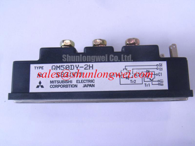
The Mitsubishi Electric QM50DY-2H is an Isolated Darlington Module with a 50 A rated collector current under the specified datasheet conditions. It is a bipolar power transistor module, not an insulated-gate bipolar transistor. For replacement assessment, the manufacturer’s terminal drawing, voltage ratings, current-rating conditions, safe operating area, and mounting instructions remain the controlling documents. An isolation test voltage must not be treated as the transistor’s collector-to-emitter voltage rating. The distinction matters immediately: base-drive requirements and charge removal cannot be taken from an IGBT gate-driver design.
Position the control-voltage measurement across the actual base and emitter connections, rather than between the base conductor and a convenient cabinet reference. As a Design Consideration, an emitter conductor carrying load current develops a transient voltage across its parasitic impedance. If the driver shares that conductor, the resulting voltage changes the effective base drive and can contaminate the feedback signal used during fault investigation.
Return-path separation is a board and wiring practice, not evidence that the QM50DY-2H contains a dedicated Kelvin emitter terminal. Where the documented terminal arrangement permits it, designers should route the driver return independently toward the emitter connection and keep load current out of that return conductor. A separate trace connected to an existing emitter terminal does not create an internally independent emitter connection; shared impedance inside the terminal arrangement still needs consideration.
Follow the outgoing base-drive conductor and its return together through the assembly. Long separation between them increases their loop area and exposure to magnetic coupling from the power conductors. During bench evaluation, compare the base-to-emitter waveform with collector current and collector-to-emitter voltage using suitable isolated or differential instrumentation. Check probe bandwidth, common-mode capability, and connection geometry before interpreting a narrow spike as genuine module behavior.
A useful troubleshooting comparison keeps operating conditions unchanged while correcting an identified external return-path problem. Observe whether the control waveform, switching transition, and protection behavior change together. Ringing that remains can involve driver output impedance, wiring inductance, transistor charge storage, or the measurement setup. Treat waveform changes as evidence to investigate, rather than assigning every oscillation to emitter coupling.
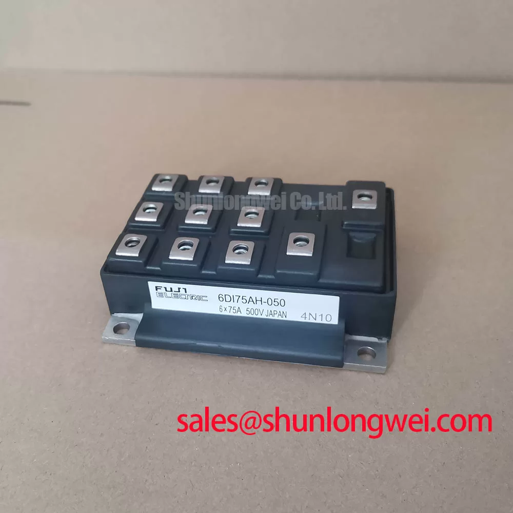
Replacement selection should preserve the original drive principle as well as the power-stage connections. The 6DI50AH-050 provides a separate product reference for a cross-comparison, not an established substitute for the QM50DY-2H. Compare device technology, circuit configuration, terminal mapping, control requirements, and mechanical interfaces before considering any redesign. Similar current markings alone do not establish interchangeability.
Keep control wiring clearance tied to the assembly’s insulation requirements and the actual surrounding conductors. Moving a return trace closer to its associated control signal can reduce coupling, but that change must not compromise separation from power terminals or exposed conductive hardware. The final routing decision belongs to the equipment design and its verified operating conditions.
Transient Dynamics & Electrical Design: Desaturation Detection on QM50DY-2H
Check collector-to-emitter voltage sensing against the Darlington’s normal conducting behavior before accepting a desaturation threshold inherited from another transistor technology. As a Design Consideration, saturation-voltage monitoring can help identify abnormal conduction, but its threshold and timing must accommodate normal switching transitions, load current, temperature, and the sensing circuit’s own response.
A fault present when the transistor is commanded on and a fault developing during conduction place different demands on the driver. The former overlaps turn-on behavior; the latter interrupts established current. Protection testing should distinguish these conditions and include the complete path from detection through driver response to current interruption. A generic short-circuit detection deadline is not a verified QM50DY-2H withstand rating.
For this Darlington module, evaluate available base-drive current, driver compliance voltage, and the reverse-current path used to remove stored charge. IGBT gate-charge sizing and gate-resistor prescriptions are not directly transferable. Any external base resistance should be assessed with the driver circuit, wiring impedance, switching losses, and measured transitions. Excessive damping can slow switching, while insufficient damping can leave the control loop sensitive to parasitic coupling.
A staged reduction of drive can be evaluated where the circuit supports controlled fault turn-off. The engineering objective is to interrupt abnormal current without creating excessive collector overvoltage or extending transistor dissipation beyond its operating boundary. The sequence, current levels, and timing must come from the actual driver implementation and safe operating area assessment. Soft turn-off terminology alone does not establish protection effectiveness.
In a regenerative braking assessment, distinguish the transistor’s switching duty from the braking resistor’s energy absorption. The resistor network, DC-link controller, and switching module have separate thermal and electrical limits. Designers considering the QM50DY-2H for an existing braking chopper should examine the original circuit’s current path, control method, and repetitive energy handling rather than assuming that the module rating establishes the subsystem’s braking capacity.
Likewise, a diode surge-current rating expressed as ITSM cannot be used as a transistor overload allowance. If the surrounding circuit contains freewheeling or rectifier devices, assess their individual surge ratings and recovery behavior separately. After a protective trip, restarting should depend on the equipment’s fault-clearance and thermal recovery criteria, not simply on the disappearance of an alarm. Review fault records before repeated energization turns an intermittent problem into sustained electrical stress.
Preventing Spurious Faults: Planar Symmetrical Busbar Geometry Guidelines for QM50DY-2H
Trace the complete switching-current loop through the DC-link capacitor, power conductors, module connections, and return path before changing a snubber. As a Design Consideration, closely coupled outgoing and returning conductors can reduce loop inductance, while unnecessary conductor length and widely separated current paths increase transient voltage during current interruption. Symmetrical geometry is useful only when it corresponds to the actual commutation paths.
The engineering relationship is that peak collector voltage includes the DC-link voltage plus the voltage developed by loop inductance during the current transition. This Engineering Calculation principle explains why a faster interruption can raise voltage stress even when the steady DC-link voltage is unchanged. It does not establish a universal inductance target for the QM50DY-2H; the acceptable layout depends on measured switching behavior and the device’s operating boundaries.
Evaluate snubber placement before changing capacitance. A capacitor connected through a long loop can leave substantial local overshoot at the transistor despite a cleaner waveform elsewhere on the bus. Candidate snubber arrangements should be checked for voltage stress, pulse-current duty, energy dissipation, and their interaction with the switching transition. Component values and clamp settings should follow the circuit assessment and bench measurements, not a package-independent rule.
Where the equipment contains several power stages, keep their functions distinct. The CM400DY-12 is a separate module reference that can be reviewed when documenting an auxiliary switching stage or another converter subsystem; it is not established here as a rectifier or a QM50DY-2H replacement. The circuit diagram determines whether a device performs switching, rectification, freewheeling, or another function.
The operating explanation in Buck Converter Step-Down Voltage Regulation is useful for understanding how switching states redistribute current between circuit paths. For maintenance assessment, that principle supports identifying the active loop during each transition. It does not establish that the QM50DY-2H assembly uses a buck topology or that a particular snubber arrangement is suitable.
If the converter feeds a long motor cable, separate transistor-terminal overshoot from reflections at the motor terminals. Those observations concern different locations and different parasitic networks. Designers should assess cable characteristics, edge behavior, motor insulation requirements, and any existing output filtering before altering the module’s local suppression network. A motor-terminal disturbance does not, by itself, prove a fault at the transistor.
Benchtop Waveform Tuning: Mitigating Stress via Common-Mode Transient Immunity on QM50DY-2H
Observe the isolated driver’s input and output during switching transitions to determine whether a reported control pulse originates before or after the isolation barrier. As a Design Consideration, common-mode displacement current can disturb the driver supply, reference path, or receiving circuit. Instrument connections also introduce coupling, so repeat suspicious measurements with a suitable probe arrangement before modifying the hardware.
The QM50DY-2H’s isolated package description does not establish reinforced insulation for an entire converter or a common-mode transient immunity rating for its driver. Assess the driver barrier, isolated power supply, connectors, board spacing, and module mounting interface as separate parts of the insulation system. Required test levels and insulation classification belong to the equipment’s applicable standards and documented design.
For compatibility assessment in a multi-megawatt offshore or onshore wind turbine full-scale converter, designers should first identify the precise subsystem and original switching technology. A power and current rating alone cannot establish suitability for the main conversion bridge. Exposure to moisture, contamination, and temperature changes also needs evaluation at enclosure and assembly level, rather than being attributed to the module package.
Review maintenance records alongside electrical waveforms. Dust-restricted cooling, deteriorated thermal interfaces, and loose external connections can change operating temperature and produce symptoms that overlap driver faults. Inspection intervals should follow the equipment maintenance plan and observed conditions. Use the documented mounting arrangement; pressure-contact hardware, spring loading, or double-sided cooling should not be assumed from the Darlington module category.
Maintenance Note: Trend terminal temperature rise and inspect the cooling airflow during scheduled service, with all physical tightening and cleaning performed only after safe isolation.
For switching disturbances associated with resonant operation, Resonant Topologies in Home Appliances provides a broader topology reference rather than a QM50DY-2H application qualification. The discussion of Zero-Voltage Switching (ZVS) Resonant Converters explains why switching conditions depend on the resonant network and timing. During fault investigation, establish whether the actual transition remains within the intended switching regime, then correlate any driver disturbance with the measured voltage transition and local supply behavior.