Content last revised on September 17, 2026
SKD145/12 Circuit Protection & Reliability: Calibrating Thermal Avalanche Margins during High Peak
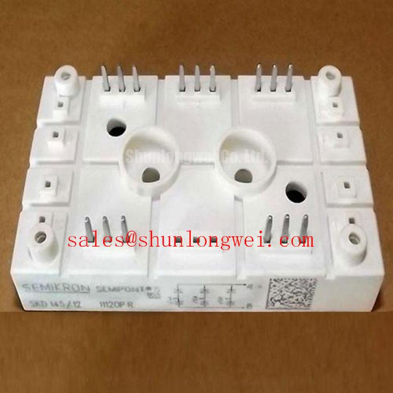
The SKD145/12 is a bridge rectifier module whose specified repetitive peak reverse voltage is 1200 V. Its factory surge capability is stated as 1800 A IFSM at Tvj = 25°C for 10 ms. This is a non repetitive surge condition, not a continuous operating current and not a substitute for protection coordination during a downstream short circuit.
For a rectifier cabinet repair, the first check is whether the event was a single supply transient, a load side fault, a loose busbar connection, or a cooling related overload. The 150°C maximum junction temperature is an Official Datasheet Specification boundary. It should be treated as a limit for verification rather than an intended operating target. A 10 ms half cycle surge can rapidly consume thermal headroom when the module begins from an elevated junction temperature.
The term ITSM is often used in rectifier protection discussions for sinusoidal surge current. For this module, the available official surge value is IFSM, so fuse coordination should be based on the module documentation, the selected semiconductor fuse time current curve, and the actual system fault path. The fuse pre arcing and clearing I²t characteristics must be assessed by the system designer against the permissible withstand data supplied for the protection scheme. No universal fuse rating can be assigned from the nominal 140 A output rating alone.
Thermal transfer also depends on a clean heatsink interface and even clamp loading. The official thermal resistance is 0.8 K/W junction to heatsink per diode. Uneven mounting pressure, oxidized contact surfaces, or a distorted heatsink can raise the effective system thermal path beyond this device level figure. ⚡ Safety Interlock Note: Isolate and discharge the DC link before loosening any module terminals or heatsink fasteners.
As a Design Consideration, inspect terminal hardware for discoloration, loss of clamping force, and evidence of repeated thermal cycling. These observations do not identify one definite failure cause, but they help determine whether a protective device, busbar assembly, cooling path, and replacement module all require review together.
Transient Dynamics & Electrical Design: RC Snubber Network Optimization to Prevent Stress on SKD145/12
The SKD145/12 rectifies current without a gate trigger terminal. Therefore, gate related turn on mechanisms and gate drive tuning do not apply to this bridge rectifier module. Its transient behavior should instead be evaluated through the AC input waveform, DC link ripple, commutation current path, transformer leakage inductance, busbar geometry, and any existing RC suppression network.
RC snubbers can be considered where measured voltage ringing or commutation related overvoltage threatens the 1200 V VRRM limit. This is a Design Consideration, not an official snubber prescription for SKD145/12. Designers should select resistor and capacitor values only after capturing voltage waveforms at the module terminals with a measurement method suitable for high energy switching circuits. The objective is to control peak voltage and ringing without placing excessive repetitive dissipation into the resistor or unacceptable reactive current into the supply.
A series saturable reactor can also be evaluated when the measured current rise places excessive stress on the rectifier, transformer, or DC link capacitors. Its suitability depends on the source impedance and load dynamics. When integrating the module into a medium frequency induction melting or hardening furnace power supply, engineers should verify the supply startup, transformer energization, and load change conditions rather than extrapolating from steady rectified current alone.
Keep the high current loop physically compact and mechanically stable to suppress inductive overshoot during current commutation. The final layout must be verified by system testing against measured peak voltage, current waveform, and temperature rise. Semikron’s SEMIPACK thyristor and diode module information provides useful product family context when reviewing power module integration practices.
Benchtop Waveform Tuning: Mitigating Stress via Gate Trigger Current Temperature Dependence on SKD145/12
Gate firing pulse rise time, back porch holding current, and multipulse triggering are relevant to thyristor controlled bridges, but they are not applicable parameters for the diode based SKD145/12 bridge rectifier. A bench evaluation should focus on the actual quantities that define this module’s operating stress: AC input voltage, phase current, DC output current, module terminal voltage, heatsink temperature, and the current sharing of parallel external paths where present.
The official forward voltage is 1.3 V maximum at IF = 150 A. This value helps estimate conduction loss at the stated test condition, but it does not establish complete cabinet dissipation. The system thermal result also includes duty cycle, ripple waveform, heatsink performance, ambient conditions, conductor losses, and airflow. Engineers should compare thermal measurements under representative loading against the allowed junction temperature boundary.
Where phase controlled equipment is being serviced upstream or downstream of the rectifier, confirm whether the waveform distortion originates in the controlled bridge, supply transformer, capacitor bank, or load. A clipped or asymmetric waveform may indicate several possible electrical or mechanical issues. Capture the waveform and compare it with the known circuit sequence before altering suppression components.
For technical troubleshooting procedures that cover controlled power assemblies as well as passive rectifier modules, the Field Engineer’s Handbook can support a structured measurement plan. Semiconductor diode behavior and technology context can also be reviewed through Semikron CAL diode technology.
SKD145/12 Thermal Electrical Optimization: Semiconductor Protection Fuse Selection in Practical Tuning
Fuse selection for SKD145/12 requires coordination of the fuse clearing characteristics with the converter topology, upstream source capability, cable impedance, and available fault energy. The objective is to limit damage during a short circuit, but an assertion of zero damage under every fault condition cannot be made from the module ratings alone. The system designer should assess fuse I²t curves, prospective current, contactor response, and enclosure protection as one fault management chain.
The bridge’s specified 3000 V a.c., 50 Hz, r.m.s. for 1 minute isolation voltage applies to the stated factory test condition. It should not be interpreted as a system insulation coordination rating, installation category, EMC certification, or proof of a complete cabinet’s dielectric performance. Verify creepage, clearance, grounding, shield termination, and enclosure requirements against the applicable equipment documentation.
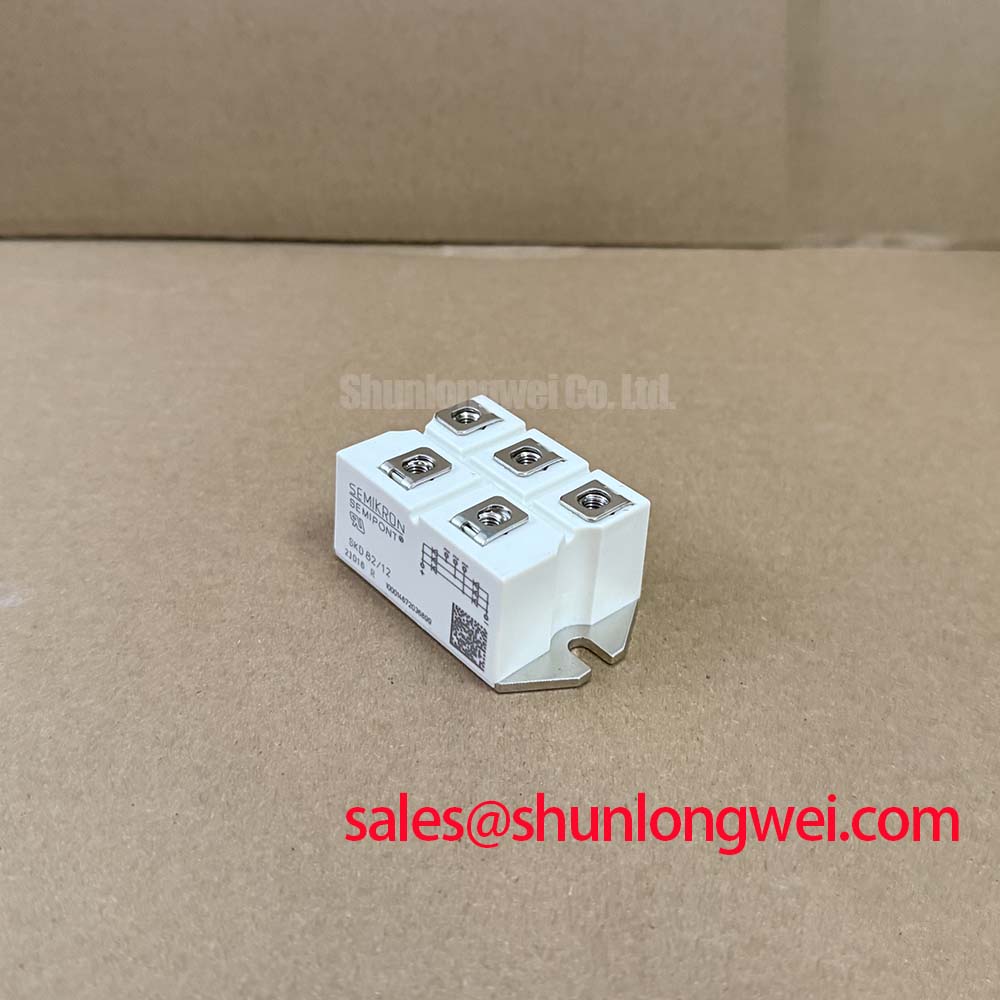
During replacement assessment, confirm that the original electrical topology requires a bridge rectifier in the SEMIPONT 5 package, then compare voltage rating, thermal interface, terminal arrangement, current duty, and protective coordination. The SKD82/18 is another Semikron bridge rectifier module that can be reviewed as a separate engineering reference; it should not be treated as an automatic substitute because its electrical and mechanical conditions must be verified against the original design.
After installation, record no load voltage, loaded current, terminal temperature trend, and the waveform across the DC link during the operating sequence. These measurements provide a practical basis for deciding whether the SKD145/12 is operating within its published electrical and thermal boundaries.