
Content last revised on June 24, 2026
Optimizing Compact Inverter Designs with the SKIIP20NAC12IT2 MiniSKiiP 2 Module
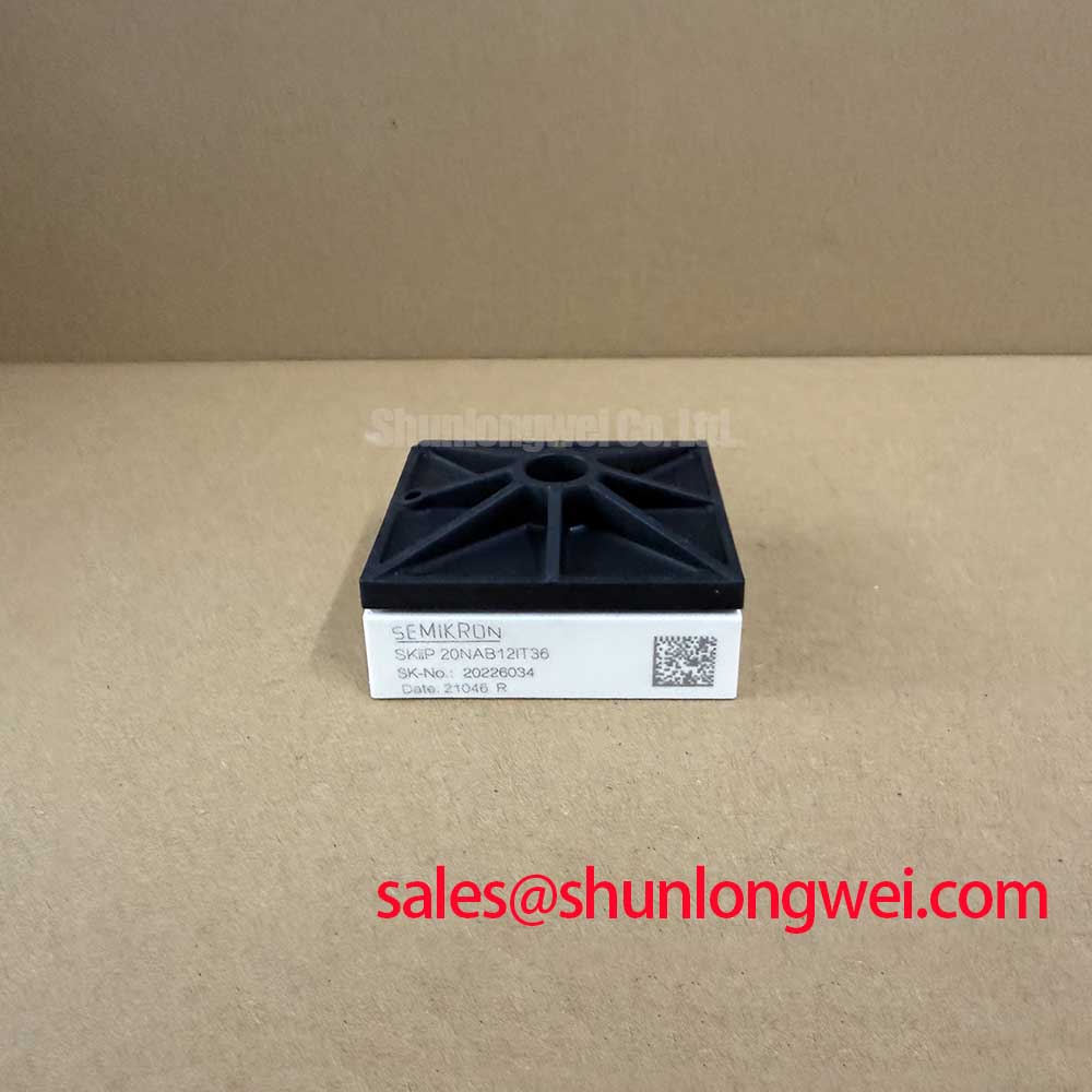
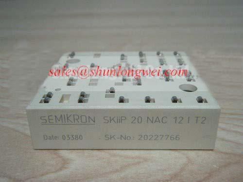
The SKIIP20NAC12IT2 represents a specialized CIB (Converter-Inverter-Brake) topology within the MiniSKiiP 2 family, designed to streamline 1200V power stage integration while maximizing thermal management efficiency. For engineers prioritizing long-term reliability in industrial motor drives, this Semikron module offers a unique solder-free pressure contact system that effectively eliminates the common failure mode of solder fatigue in high-cycle applications. Delivering 21A of collector current at 25°C, it provides a robust foundation for compact Variable Frequency Drives (VFD) and servo drive systems. What is the primary benefit of the SKIIP20NAC12IT2 pressure contact technology? It dramatically enhances power cycling capability by replacing rigid solder joints with flexible, spring-loaded mechanical connections. For 400V AC grid systems requiring a CIB configuration in a minimized footprint, the SKIIP20NAC12IT2 is the high-density choice for modern power electronics design.
Key Parameter Overview
Decoding the Specs for Enhanced Thermal Reliability
The following table summarizes the critical electrical and thermal limits of the SKIIP20NAC12IT2 based on its official technical documentation. These values are essential for calculating system-level efficiency and designing appropriate thermal management solutions.
| Parameter | Symbol | Typical Value | Unit |
|---|---|---|---|
| Collector-Emitter Voltage | Vces | 1200 | V |
| Collector Current (Ts = 25°C) | Ic | 21 | A |
| Collector Current (Ts = 70°C) | Ic | 15 | A |
| Vce(sat) (Ic = 15A, Tj = 25°C) | Vce(sat) | 1.70 | V |
| Maximum Junction Temperature | Tj(max) | 175 | °C |
| Integrated NTC Sensor | R25 | 1000 | Ω |
| Package Type | MiniSKiiP 2 | CIB | - |
Download the SKIIP20NAC12IT2 datasheet for detailed specifications and performance curves.
Application Scenarios & Value
Achieving System-Level Benefits in High-Frequency Power Conversion
In the realm of industrial automation, the SKIIP20NAC12IT2 is frequently deployed in Variable Frequency Drives (VFD) and Servo Drives where space and reliability are non-negotiable. A significant engineering challenge in these systems is managing the thermal stress caused by rapid load changes. By utilizing Trench IGBT3 technology, the SKIIP20NAC12IT2 reduces Switching Loss significantly compared to older planar structures.
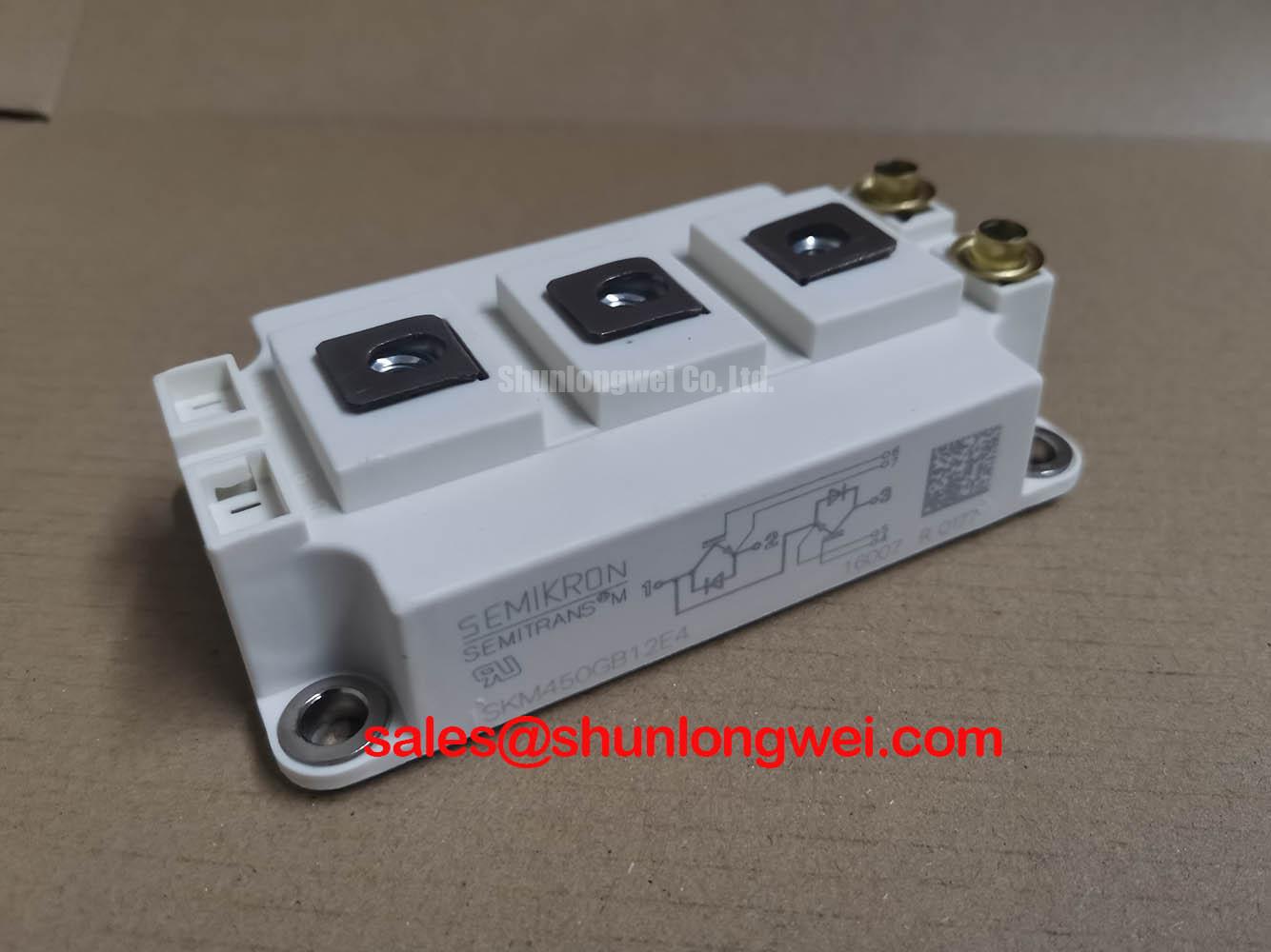
Consider a multi-axis robotic controller operating in a high-ambient-temperature factory environment. The integrated brake chopper and three-phase rectifier bridge allow for a complete power stage within a single MiniSKiiP 2 module. This high level of integration simplifies the PFC stage design and reduces parasitic inductance, which is critical for maintaining signal integrity at higher switching frequencies. While this module is ideal for mid-power precision control, for systems requiring significantly higher current handling, the related SKIIP 35NAB126V1 offers a higher Ic rating within a similar architecture.
The SKIIP20NAC12IT2 is also an excellent fit for industrial fan and pump controllers where the TCO (Total Cost of Ownership) is prioritized. The solder-free assembly reduces manufacturing complexity, allowing for a design simplification that speeds up time-to-market. For guidance on verifying these modules in the field, see our guide on how to test an IGBT module with a multimeter.
Technical Deep Dive
The Engineering Logic Behind Pressure-Contact Technology
The most defining characteristic of the SKIIP20NAC12IT2 is its departure from traditional soldering. In a standard IGBT Module, the chips are soldered to a substrate, which is then soldered to a baseplate or directly to a PCB. Over thousands of power cycling events, the mismatched coefficients of thermal expansion (CTE) between these layers cause the solder to crack—a phenomenon known as solder creep or fatigue.
The SKIIP20NAC12IT2 utilizes Semikron pressure-contact technology, which can be likened to a high-tension suspension system in a performance vehicle. Instead of a rigid, brittle permanent bond, the electrical and thermal connections are maintained by a precisely calibrated mechanical force. This "spring-like" interface absorbs thermal expansion and contraction without degrading the electrical path. This results in an order-of-magnitude improvement in reliability for UPS (Uninterruptible Power Supply) and solar inverter applications that experience constant thermal flux.
Furthermore, the Vce(sat) of 1.70V indicates an optimized balance between conduction losses and switching speed. For a deeper understanding of these trade-offs, engineers can refer to our analysis of IGBT vs. MOSFET vs. BJT. Additionally, the MiniSKiiP 2 package's low Thermal Resistance is a direct result of the direct-pressed ceramic substrate, which provides a shorter thermal path to the heatsink compared to modules with thick copper baseplates. This physical structure is explored further in our resource on why Rth matters in power design.
Frequently Asked Questions
- How does the pressure-contact design of the SKIIP20NAC12IT2 impact PCB assembly?
Unlike traditional modules, the SKIIP20NAC12IT2 does not require wave or hand soldering. It is pressed onto the PCB using a single-screw mounting system. This requires specific PCB pad plating (typically electrolytic gold or HAL) to ensure a gas-tight, low-resistance contact over the life of the product. - Can the integrated NTC sensor be used for real-time over-temperature protection?
Yes. The 1000 Ω NTC sensor is thermally coupled to the internal IGBT chips. It is designed to provide accurate temperature feedback to the Gate Drive controller, allowing the system to implement derating or emergency shutdown procedures before the junction reaches the 175°C limit, thereby preventing catastrophic failure.
The SKIIP20NAC12IT2 remains a strategic choice for OEMs looking to bridge the gap between high-performance switching and industrial-grade durability. By leveraging the CIB topology and MiniSKiiP's unique mechanical advantages, designers can achieve higher power densities without compromising on the expected service life of the inverter.