Content last revised on October 12, 2026
SKIIP30NAB12T49 Product Overview and Pre-Energization Checks
- Record cold state resistance and isolation readings at the main power and control interfaces before energizing the drive, using test methods compatible with the connected electronics.
- Check the mounting surface, heatsink flatness, thermal interface condition, and airflow path for contamination or obstruction.
- Confirm the gate driver wiring, auxiliary supply sequence, UVLO interlock, and isolation barriers against the original drive documentation.
- Inspect mounting hardware and electrical contacts for correct assembly and evidence of mechanical loading around the power connections.
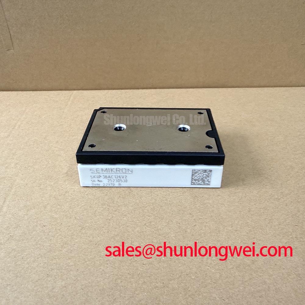
SKIIP30NAB12T49 is a Semikron IGBT power module in the MiniSKiiP package family, in the 1200 V, 30 A class. The voltage and current ratings identify the electrical class of the device, but the allowable operating point in a CNC servo or robotic drive remains dependent on the datasheet rating conditions, switching frequency, cooling conditions, current waveform, overload profile, and the complete gate driver design.
| Manufacturer | Semikron |
| Part number | SKIIP30NAB12T49 |
| Product category | IGBT power module |
| Voltage class | 1200 V |
| Current class | 30 A; allowable current depends on the specified conditions |
| Package family | MiniSKiiP |
For a replacement review, compare the complete electrical topology rather than matching only the voltage and current printed on the label. Confirm the original control board interface, protection behavior, power connection arrangement, thermal mounting method, and switching requirements. The Semikron resources on MiniSKiiP® Power Modules and SKiiP® Technology provide useful background for evaluating the package family and its integration approach.
Transient Dynamics & Electrical Design: Regenerative DC Bus Voltage Surge Dissipation on SKIIP30NAB12T49
Regenerative energy from a rapidly decelerating motor should first be traced through the actual DC bus topology before any braking component is selected. In a high dynamics multi axis CNC or robotics servo, the motor can return energy through the inverter into the DC link. The resulting bus rise is influenced by motor speed, deceleration command, mechanical load, capacitor condition, braking duty, and the switching path inductance. The 1200 V voltage class of the SKIIP30NAB12T49 is not a permission to operate the complete drive at that voltage during every transient condition.
A practical commissioning review begins at the DC link measurement points. Use a suitably rated differential probe and capture the bus voltage during the fastest expected stop, controlled deceleration, and repeated motion cycle. The oscilloscope record should distinguish the normal regenerative rise from narrow switching overshoot. Long probe leads and temporary wiring can add misleading ringing, so the measurement loop should be short and positioned according to the drive manufacturer’s safety procedure.
The braking IGBT and ballast resistor must be dimensioned from the machine’s regenerated kinetic energy, allowable DC bus window, pulse repetition, resistor thermal behavior, and the cooling available inside the cabinet. If the SKIIP30NAB12T49 is being evaluated in a braking path, verify that its actual internal topology and driver interface match the circuit under review. Do not infer an internal braking channel, resistor interface, or a particular regenerative control method from the product family name alone.
MOV coordination is a system level protection task. The selected MOV network should clamp abnormal energy without creating an operating point that conflicts with the DC bus insulation system, semiconductor voltage rating, or fuse coordination. Its energy capability, repetitive duty, leakage at normal bus voltage, and thermal disconnection behavior require review as part of the cabinet protection design. The MOV is not a substitute for correct braking control, adequate DC link capacitance, or a properly rated semiconductor switch.
Where a rectifier or front end shares the same energy path, the surrounding topology should be checked as a complete chain. A device such as SK30GD123D may be evaluated as an associated power-stage component when its documented topology, electrical role, voltage class, current waveform, and control method are compatible with the equipment. This is a neutral topology reference, not a universal replacement recommendation.
Surge current review also needs to separate repetitive operating current from an abnormal inrush or fault event. For rectifiers and other devices with a specified ITSM rating, that capability, fuse clearing behavior, DC link precharge sequence, and junction temperature recovery window should be taken from the applicable device documentation and the complete drive protection study. IGBT fault capability must be assessed using its own documented limits. A short high current event can impose a different thermal and mechanical stress profile from a steady 30 A operating condition.
For a resistor or braking switch that repeatedly absorbs deceleration energy, inspect the waveform at the switch terminals and across the resistor. Look for delayed turn on, excessive bus overshoot, resistor hot spots, and a duty cycle that changes as the cabinet temperature rises. The control system should be tested at the most demanding motion profile available, with the bus voltage and braking current recorded together. This establishes whether the observed limit comes from the braking branch, the DC link, the control timing, or the mechanical load.
Transient Dynamics & Electrical Design: Preventing Mechanical Damage during SKIIP30NAB12T49 Installation
Mechanical installation directly affects the electrical reliability of a power module because uneven loading can transfer force into internal conductors and package interfaces. Before securing the assembly, place the module on a clean, suitable heatsink surface and verify that the fasteners draw the package down evenly. The correct mounting torque must come from the applicable Semikron mechanical documentation and the cabinet assembly standard; do not infer it from the electrical rating.
The MiniSKiiP spring-contact interface requires correct PCB alignment, contact-pad condition, and assembly compression rather than tightening individual module power-terminal screws. Follow the applicable assembly instructions for the module, PCB, and mounting hardware. Where external screw-connected busbars are used elsewhere in the assembly, thread engagement should be sufficient without allowing the fastener to bottom out. Correct busbar alignment mechanically before tightening so that loading is not transferred into the PCB or module contacts.
Thermal cycling makes this inspection important even when the initial electrical test is normal. Copper conductors, busbars, fasteners, thermal interfaces, and heatsinks expand at different rates. Repeated heating and cooling can alter contact conditions or shift a rigid connection. During preventive maintenance, inspect for discoloration, loosened hardware, damaged insulation, and a change in connection temperature relative to neighboring phases. Temperature comparison is a useful condition indicator, but it should be interpreted with the same load and airflow conditions.
⚠️ Maintenance Note: Keep the heatsink and fan path free of dust, and recheck thermal interface condition whenever contact temperature rises under a previously stable machine load.
Short circuit protection requires a separate electrical review. A desaturation circuit can detect an abnormal rise in collector emitter voltage during conduction, but its response depends on the gate driver, blanking behavior, sensing path, noise immunity, and the device’s switching state. A sub three microsecond protection target and two stage soft turn off are design considerations sometimes used in fast IGBT protection, not official SKIIP30NAB12T49 ratings. The driver designer must verify the actual timing against the device’s documented short circuit limits, the selected gate driver, and the measured fault waveform.
In a two stage soft turn off arrangement, the first action limits the rate of current change while the second action completes gate discharge under controlled conditions. The intention is to reduce the voltage overshoot associated with interrupting fault current. The appropriate timing and gate impedance are system determined. They should be validated with isolated probing, controlled fault testing, and a review of peak collector emitter voltage against the device’s documented limits.
Fast semiconductor fuses should be coordinated using the applicable I²t data, prospective fault current, DC bus voltage, wiring inductance, and clearing time. Where suitable withstand data are available, check whether fuse clearing can protect the relevant semiconductor path. A fuse must not be assumed to protect an IGBT against a fast short circuit; rapid gate-driver protection is also needed. A fuse label alone does not establish protection for a particular installation. Check the complete fuse, busbar, contactor, precharge, and module arrangement.
The freewheel path also deserves attention. If the inverter topology includes a diode, its reverse recovery softness affects voltage overshoot, common mode current, and radiated EMI. The relevant softness factor, reverse recovery charge, switching temperature, and commutation loop must be assessed from the actual diode and operating conditions. These characteristics should not be assigned to the SKIIP30NAB12T49 without a matching device specification.
Field Diagnostics & Commissioning: Gate Driver Auxiliary Power Sequencing in SKIIP30NAB12T49 Topologies
Apply the gate driver auxiliary supplies and verify the UVLO interlocks before connecting the high voltage DC link, following the drive manufacturer’s commissioning sequence. The control sequence should prevent PWM commands from reaching the power stage while the driver supply is rising, falling, or outside its valid operating region. A clean commissioning record includes the auxiliary supply waveform, enable signal, fault output, gate emitter voltage, and DC link timing on a shared time base.
A negative turn off bias may be used in some IGBT driver arrangements as a design consideration for noise immunity and controlled turn off. No particular negative bias is specified for the SKIIP30NAB12T49 here. The system integrator must verify the permitted gate emitter voltage, driver output capability, isolation rating, and the exact gate network from the relevant device and driver documentation before applying negative bias.
Gate resistance should be treated as part of the switching loop, not as an isolated component value. Excessive resistance can slow turn on or turn off and increase switching losses; insufficient damping can intensify ringing and false triggering. During commissioning, inspect the gate waveform at the module terminals with a properly isolated probe. Compare the command signal, gate voltage, collector emitter response, and driver fault signal during both light load and the highest practical operating load.
Protection timing must also account for auxiliary power collapse. When the driver supply falls through its UVLO region, the gate output should move to the intended safe state without leaving a partially enhanced device. Confirm this behavior during controlled power removal and controller reset tests. The result should be checked for every relevant phase and switching position rather than inferred from a single channel.
For topologies using a thyristor or controlled rectifier elsewhere in the power path, gate trigger current, gate trigger voltage, and pulse train strength belong to that specific device and its driver. A repeated trigger pulse can help ensure triggering in some circuit arrangements, but the pulse amplitude, width, repetition, and isolation must be selected from the thyristor data and control architecture. These characteristics should not be presented as specifications of the SKIIP30NAB12T49 IGBT power module.
Parallel semiconductor paths require both static and dynamic current sharing analysis. A positive temperature coefficient can assist sharing in some operating regions, yet layout symmetry, gate loop impedance, thermal coupling, switching delay, and device spread still influence the result. The engineer should measure phase current and switching waveforms at the intended temperature range instead of assuming that identical part markings guarantee equal dynamic current.
For service planning, record the module identification, heatsink condition, connection temperature, driver fault history, and DC link waveform under a repeatable machine cycle. When comparing a candidate device such as SKIIP12AC126V1, compare topology, ratings, control interface, package mechanics, and protection behavior as separate checkpoints. Broader application context for industrial inverter, renewable energy, and heavy duty power systems is available in the Industrial Applications reference.
Potential equipment evaluation may include high dynamics multi axis CNC servo drives, robot joint amplifiers, and compact industrial motion cabinets, subject to the original system documentation and thermal design. Before returning equipment to service, verify insulation, auxiliary sequencing, gate behavior, protective shutdown, cooling airflow, and DC bus response under a controlled commissioning procedure.