




Content last revised on September 17, 2026
SKIIP38AC126V2 Circuit Protection & Reliability: Calibrating and Suppressing Cres-Induced Gate Voltage Spikes
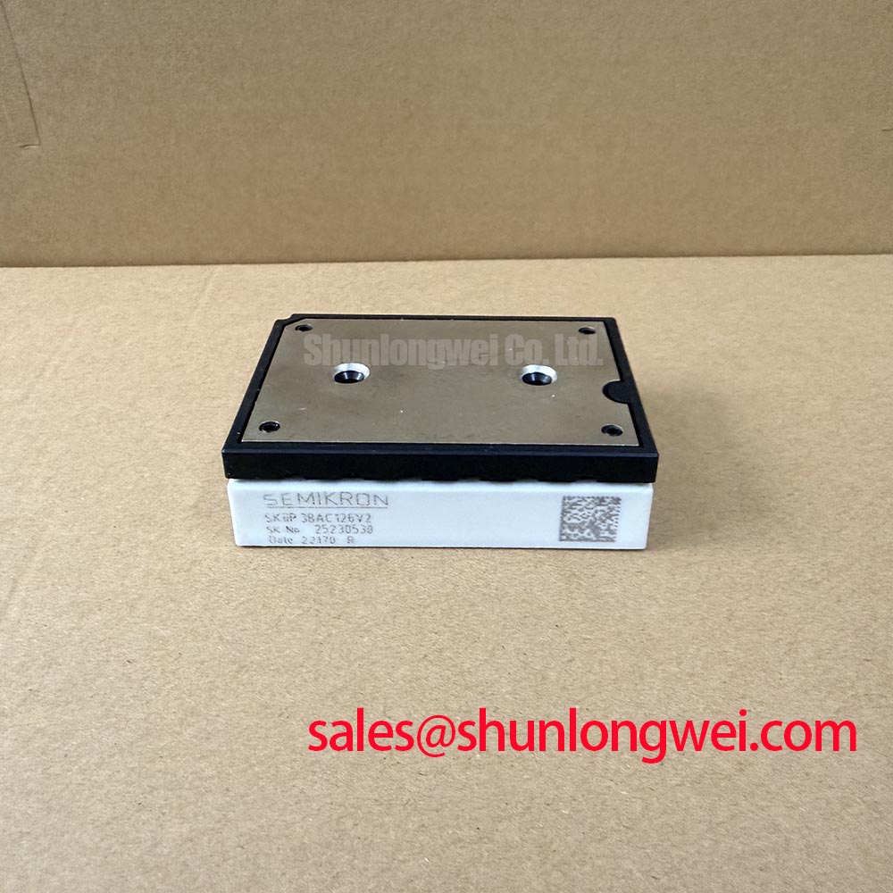
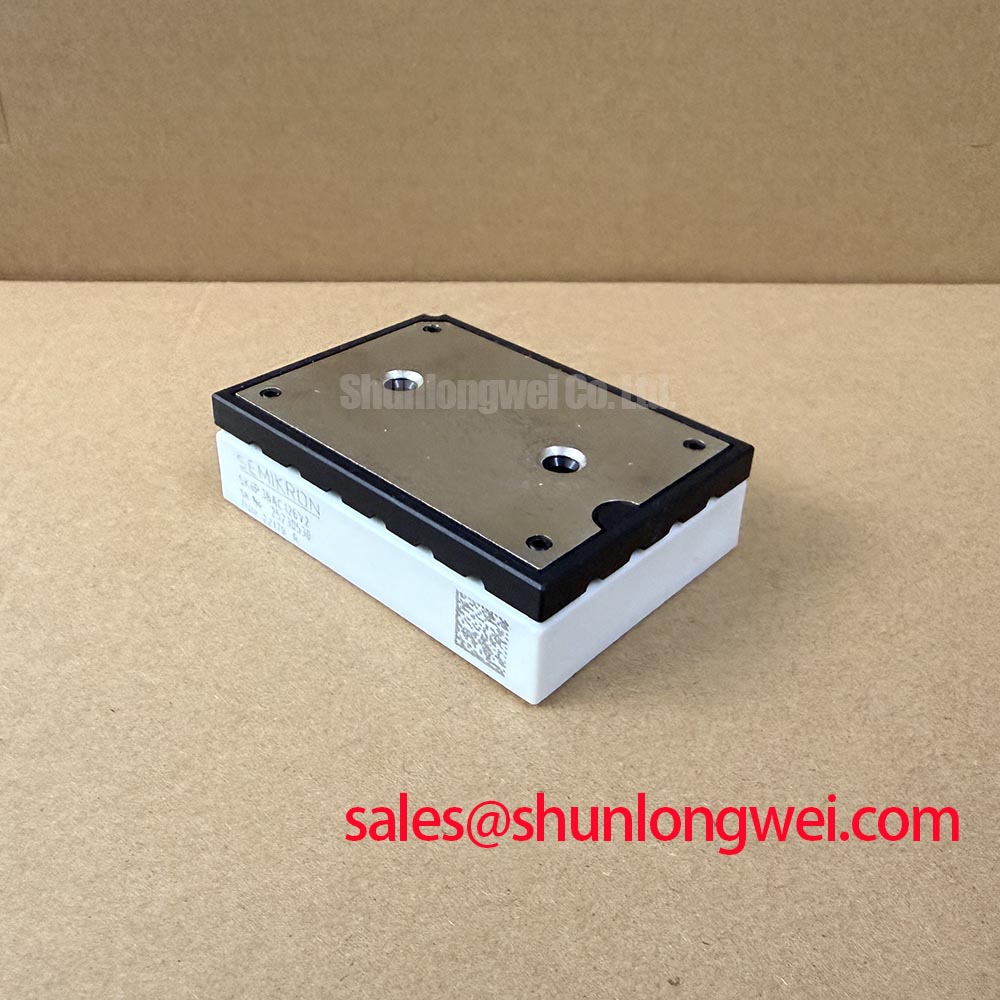
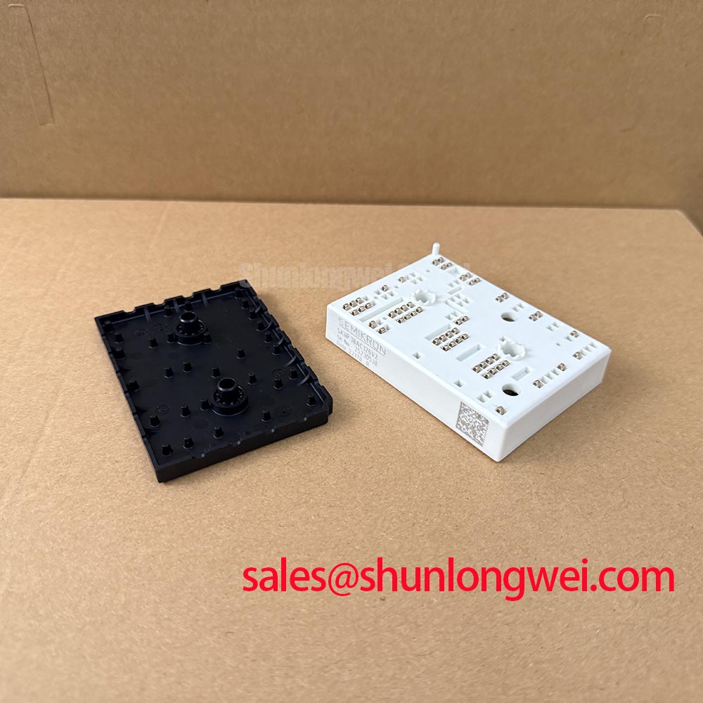
Begin incoming inspection by confirming the enclosure marking and checking power and control terminals against the original equipment connection diagram with the assembly fully isolated. The SKIIP38AC126V2 is a Semikron intelligent power module specified at VCES = 1200 V and ICnom = 100 A at a heatsink temperature of 25 degrees C. Its stated insulation rating is Visol = 2500 V AC for 1 minute, which is an Official Specification and should be evaluated against the complete equipment insulation scheme rather than treated as a complete system safety certification.
| Official Specification | Condition | Value |
|---|---|---|
| Collector emitter voltage | Tj = 25 degrees C | 1200 V |
| Nominal inverter collector current | Ts = 25 degrees C | 100 A |
| Collector emitter saturation voltage | IC = 100 A, Tj = 125 degrees C | 1.7 V typical |
| Junction to heatsink thermal resistance | Per IGBT | 0.40 K/W |
| Short circuit withstand time | VCC = 800 V, Tj less than or equal to 150 degrees C | 10 microseconds |
| Isolation voltage | AC, 1 minute | 2500 V |
During switching, collector voltage transitions can couple through device capacitances into an inactive gate loop. A Design Consideration is to inspect the gate return path, active Miller clamp function, driver supply reference, and gate loop symmetry before raising DC link voltage. A low impedance clamp path can limit unintended gate rise during high dv/dt events, while the appropriate negative gate bias must be qualified by the system engineer against the installed driver and module documentation.
Keep high current commutation paths compact and place the DC link connection so parasitic inductance is minimized. This is an Engineering Recommendation for suppressing turn off overshoot, with the resulting voltage margin verified using appropriately rated differential measurement equipment during switching tests. For product-family context, the manufacturer describes the MiniSKiiP platform at Semikron MiniSKiiP Power Modules.
💡 Bench Tip: Record cold-state diode-mode and insulation-test observations from a known-good assembly before comparing a replacement module, and maintain ESD controls whenever handling control terminals.
Benchtop Waveform Tuning: Mitigating Stress via Derating Guidelines and Mismatched Parameters on SKIIP38AC126V2
At 100 A and a junction temperature of 125 degrees C, the official typical collector-emitter saturation voltage is 1.7 V. This parameter helps estimate conduction behavior at the stated test condition, but it does not establish total inverter loss at a particular switching frequency, cooling condition, modulation strategy, or load profile. Designers should evaluate conduction and switching waveforms in the actual converter before defining the permitted operating envelope.
Positive temperature behavior of IGBT saturation voltage can assist steady-state current sharing in parallel paths, yet dynamic current balance still depends on matched gate wiring, matched driver behavior, and similar commutation conditions. A Design Consideration is to compare turn-on and turn-off waveforms across corresponding legs. A difference may indicate unequal gate-loop impedance, nonuniform DC-link geometry, driver timing variation, or another system-level condition requiring measurement.
Freewheeling-diode reverse recovery can sharpen the commutation transient and contribute to radiated noise. Engineers can assess whether a snubber network, revised busbar arrangement, or changed gate damping is appropriate by measuring collector-emitter voltage and current together on the existing hardware. The objective is to control ringing and peak stress without assuming that a single resistor value applies to every inverter.
For an equipment-level comparison where electrical and mechanical documentation is available, SKIIP37AC12T4V1 provides a related reference point. Terminal assignment, control interface, protection behavior, thermal interface, and system qualification remain items to verify rather than assumptions for interchangeability. In systems using a separate power stage, SKM100GB063D is a neutral reference for reviewing the surrounding rectifier or complementary switching topology.
Field Diagnostics & Commissioning: Baseplate Convexity Compensation and Screw Torque in SKIIP38AC126V2 Topologies
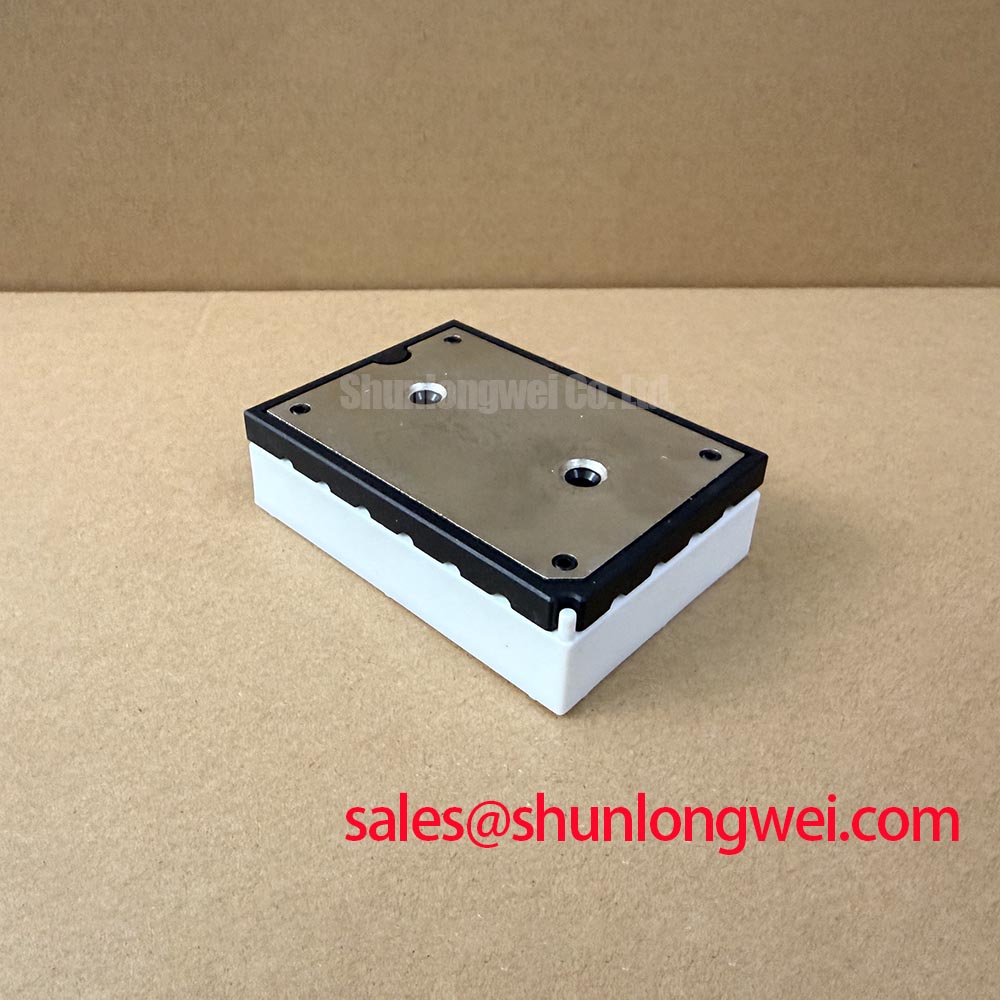
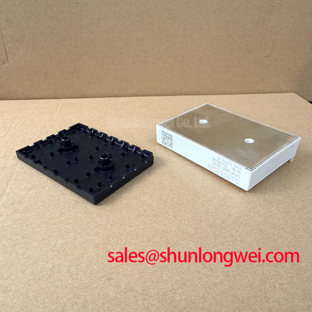
Before installation, inspect the heatsink contact area for debris, machining damage, corrosion, and evidence of uneven prior contact. The official junction-to-heatsink thermal resistance is 0.40 K/W per IGBT; it is a device specification, while installed thermal performance also depends on heatsink flatness, interface material coverage, clamp loading, airflow, and the measured load cycle.
A Design Consideration is to apply thermal interface material as a controlled, continuous layer and remove trapped voids without allowing excess material to distort seating. In common power-module assembly practice, a thin TIM layer in the 50 to 100 micrometre range is often evaluated, but the appropriate material and final thickness must be set by the heatsink surface condition and the equipment manufacturer requirements.
Where a baseplate or mounting plane shows measurable curvature, use the specified screw sequence and tighten progressively to distribute pressure. Do not attempt to correct a mechanical mismatch by concentrating force at one location. After commissioning, compare heatsink temperature trends, load current, switching waveform behavior, and protective-event records with a known-good unit. These observations can distinguish several possible installation, cooling, driver, or load-related causes without assigning a single cause from one symptom.
⚠️ Field Alert: Disconnect and verify discharge of the DC link before removing control or power connections, because stored energy can remain hazardous after the controller is switched off.
SKIIP38AC126V2 Operational Boundaries: Evaluating Bi-Directional DC-DC Buck-Boost Conversion Limits
When a commercial string inverter or micro-grid energy-storage system is assessed for bidirectional power transfer, the 1200 V voltage rating and 100 A nominal inverter-current rating define important official boundaries for the module. They do not independently approve a four-quadrant battery interface. The integrator should verify DC-link limits, switching transient peaks, protection response, battery management limits, and the converter control sequence on the complete assembly.
The stated short-circuit withstand time is 10 microseconds at VCC = 800 V and junction temperature no higher than 150 degrees C. This is an Official Specification test condition, not a recommended protection delay. Protection coordination should be validated from the actual fault-detection chain, gate-drive shutdown behavior, DC-link energy, semiconductor fuse characteristics, and fault current path. A fast fuse selection must be assessed using its published time-current and I squared t information together with the system fault study.
Peak-shaving duty can impose repeated thermal changes as battery current reverses and inverter loading moves between charge and discharge. Designers should calculate junction-temperature excursions using the applicable transient thermal impedance information and then verify the result with representative duty-cycle measurements. Cooling-path integrity, gate-drive stability, and DC-link overshoot deserve review at both power-flow directions.
For broader technology context when comparing IGBT-based power stages with other semiconductor approaches, see Wide Bandgap Revolution. Any change in semiconductor technology, topology, or switching strategy requires separate electrical, thermal, insulation, and control validation.