



Content last revised on September 22, 2026
Incoming Inspection and Device Specifications
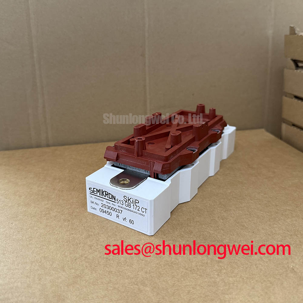
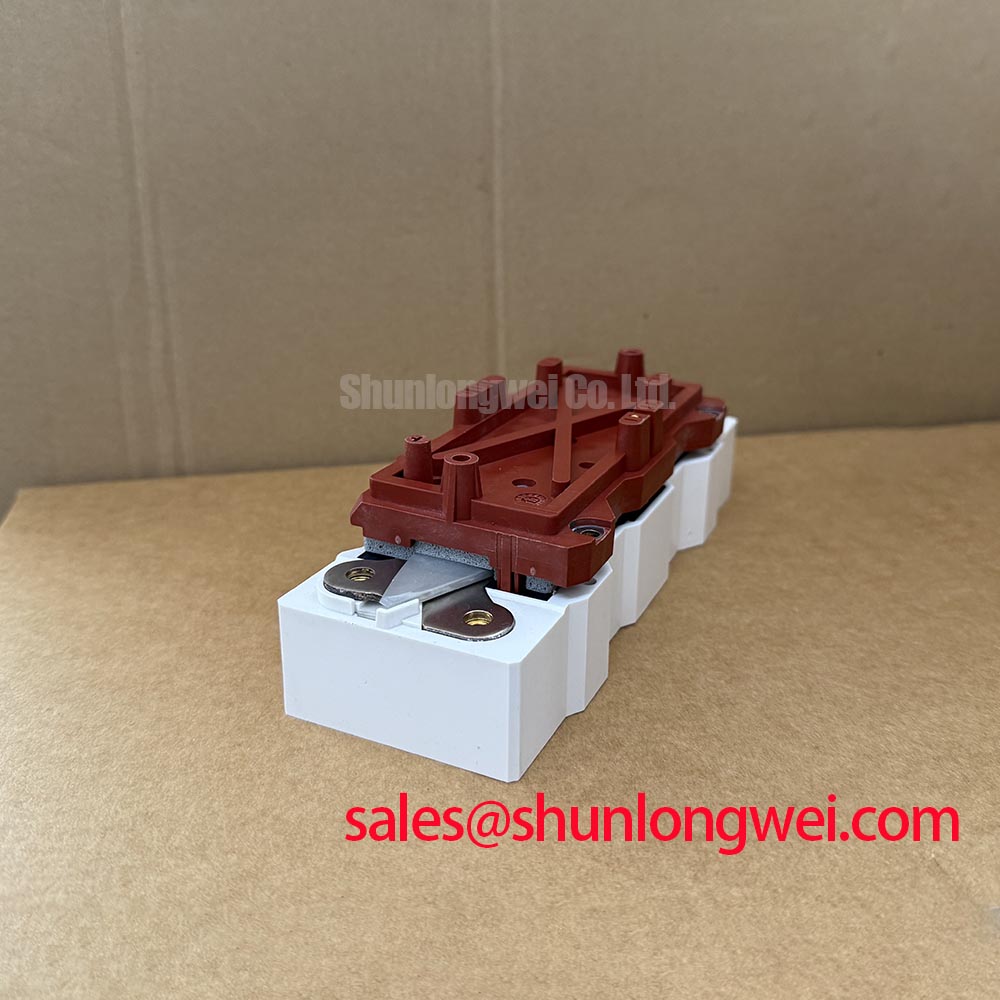
Begin incoming inspection by isolating the SKIIP513GB172CT, recording its marking, checking the pressure contact surfaces for visible damage, and verifying the circuit position against the equipment schematic before applying any test voltage. Use an ESD controlled bench, confirm the power terminals and gate control connections from the original module documentation, and perform cold state resistance and diode mode checks only with the module fully disconnected.
| Parameter | Official Specification |
|---|---|
| Manufacturer | Semikron |
| Module type | IPM power module |
| Topology | Half Bridge |
| VCES | 1700 V |
| Nominal collector current | 500 A |
| Thermal technology | Baseplate less pressure contact |
| Integrated protection functions | Over current, over temperature, and under voltage lockout |
These values are official product data supplied for this device. They should not be treated as a complete operating envelope for a finished inverter. Switching frequency, gate drive voltage, short circuit withstand behavior, thermal impedance, isolation capability, and allowable overload duration must be confirmed from the applicable Semikron documentation and the installed system design.
Benchtop Waveform Tuning: Mitigating Stress via Common Mode Transient Immunity in Harsh Switching Conditions
For a 1500 V class central photovoltaic inverter, begin waveform work with the gate driver disabled and confirm that the module control terminals remain at their intended inactive state. The half bridge topology places strong demands on driver timing because a false command during DC link energization or regenerative braking can create simultaneous conduction. Verify the actual signal path with an isolated oscilloscope arrangement suitable for the common mode voltage present in the test fixture.
Common mode transient immunity is a system level design consideration rather than an automatic specification of this module. Designers should verify the required galvanic isolation rating and transient immunity of the selected gate driver, power supply, signal isolator, and measurement equipment. The control loop should minimize parasitic coupling between the high power commutation path and the gate return path. Clearance and creepage distances must be selected according to the working voltage, pollution environment, insulation system, and applicable safety standard.
During bench tuning, compare the high side and low side gate waveforms with the DC link disabled first, then repeat the measurement under controlled switching conditions. Unexpected gate movement may indicate coupling, probing error, driver supply disturbance, or an incorrect return path. Check each possibility against a known good signal path rather than assigning the symptom to the module alone.
💡 Bench Tip: Keep the module, driver board, and oscilloscope reference under ESD control, and record the cold state diode test results before any powered waveform experiment.
Assembly Integrity and Layout Architecture: Thermal Time Constants and Peak Junction Evaluation
The baseplate less pressure contact construction makes assembly consistency important. The mechanical interface, pressure distribution, contact cleanliness, cooling structure, and electrical bus arrangement should be checked against the manufacturer’s installation instructions. A pressure contact module should not be evaluated by visual seating alone; the equipment builder must verify the specified clamping method and confirm that the cooling path remains uniform across the active area.
For regenerative braking choppers and high power braking resistor systems, the thermal calculation should distinguish short pulse overload from continuous dissipation. The engineering model normally combines the module’s junction to case response with the cooling assembly response, then compares the calculated junction temperature against the applicable device rating. The time constants and thermal impedance data must come from the relevant Semikron documentation. They cannot be inferred from the 1700 V and 500 A headline ratings.
In a bidirectional DC DC battery interface, repeated charge and discharge pulses can produce thermal cycling at the semiconductor, contact, and cooling interfaces. Designers should evaluate the mission profile, pulse repetition, ambient conditions, and cooling transient response before assigning a service life expectation. No field life or failure rate should be assumed without a documented test source.
Fuse coordination also requires a direct comparison between the semiconductor fuse clearing characteristic, the module short circuit capability, and the system’s available fault energy. Verify the selected fuse I2t relationship and clearing sequence with controlled tests. The thermal packaging background can be reviewed through The Advanced Thermal Management Revolution, while general information on high temperature PPS packaging is available from Polyphenylene Sulfide.
Transient Dynamics and Electrical Design: High dv/dt Cross Conduction and Shoot Through
High dv/dt switching can couple through the gate loop and create a temporary command on the inactive device. This is a design consideration for any half bridge and should be investigated by observing both gate to emitter voltage waveforms during the fastest normal switching event. The measurement circuit must have low loop inductance and sufficient bandwidth so that probe artifacts are not mistaken for a gate disturbance.
A dedicated low impedance gate loop, controlled turn on and turn off behavior, and an active Miller clamp may help reduce unwanted gate movement when supported by the selected driver architecture. Negative gate bias is not an automatic requirement for this module. If the system designer considers it, the permitted gate voltage range, driver isolation, power supply behavior, and gate oxide limits must first be confirmed from the official device and driver documentation. The final value remains system determined and requires bench validation.
Dead time should be established from measured turn off, propagation delay, driver asymmetry, temperature, and load current behavior rather than copied from an unrelated module. In a braking chopper, inspect the transition between energy absorption and freewheel paths. In a bidirectional battery converter, repeat the test in both power flow directions because commutation conditions can change with current polarity.
The Semikron MiniSKiiP power module reference provides useful manufacturer context for module integration, but the applicable electrical and mechanical data for the SKIIP513GB172CT must be taken from its own documentation.
Hard Switching Transients: Short Circuit Detection and Controlled Turn Off
The integrated protection description for the SKIIP513GB172CT includes over current, over temperature, and under voltage lockout. These functions should be treated as part of the module interface and verified with the correct control circuit. Their presence does not remove the need for external fault sensing, gate driver coordination, DC link protection, and an appropriate semiconductor fuse where required by the equipment architecture.
Short circuit response time, short circuit safe operating behavior, and the suitability of a two stage soft turn off must be confirmed from the official Semikron data. Do not assume a response under a particular microsecond limit without a published specification. The preferred test method is a controlled low energy fault test followed by a review of collector emitter voltage, current decay, gate voltage, driver supply stability, and clamping behavior.
Hard turn off can generate inductive overvoltage from the commutation loop. Minimize the power loop inductance, position the snubber and clamp network according to the switching topology, and verify peak voltage against the module’s rated boundary during actual switching tests. The system engineer should also inspect the DC link capacitor connection, busbar symmetry, gate return routing, and fault detector delay as a combined network.
For a utility scale 1500 V high power central solar photovoltaic inverter, this module may be evaluated where its 1700 V voltage rating, 500 A nominal current, half bridge topology, and integrated protection functions match the equipment requirements. Any alternative such as SKIIP37AC12T4V1 requires an independent electrical, mechanical, thermal, and control interface comparison before consideration as a replacement.