


Content last revised on October 1, 2026
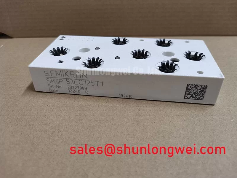
SKIIP83EC125T1 Thermal and Electrical Checks: Common Mode Transients
| Hardware specification | Official Specification |
|---|---|
| Model | SKIIP83EC125T1 |
| Manufacturer | Semikron |
| Product category | Intelligent power module |
| Voltage rating | 1200 V |
| Current rating | 83 A |
| Package family | SKiiP |
Measure resistance between each accessible power terminal and the mounting interface on the unpowered assembly, then compare the readings with the equipment’s incoming inspection record. A handheld meter can expose an obvious short or contamination path, but it cannot establish the module’s insulation withstand rating. Do not infer a galvanic isolation voltage or a common mode transient immunity rating for SKIIP83EC125T1 from its 1200 V blocking rating; those are different specifications. An insulation withstand test belongs to an approved procedure with the correct test points, limits, and precautions for the assembled equipment.
For incoming static inspection, identify the power and control contacts from the equipment wiring diagram and the applicable module pinout before placing meter probes. Record cold diode mode readings in both directions across each documented power path. Compare polarity and relative readings with a known good assembly measured under the same conditions rather than assigning a universal forward voltage threshold. A parallel circuit, charged capacitor, or connected driver can change what the meter displays, so isolate the module from surrounding circuitry where the service procedure permits.
💡 Bench Tip: Discharge the DC link and protect exposed control contacts from electrostatic discharge before comparing cold diode readings.
If an inverter reports an unexpected gate event during a fast switching transition, capture the gate signal and the relevant power node with measurement equipment suited to the installation. A coincident disturbance may point toward coupling through the driver supply, control return, or nearby high current conductors; the waveform alone does not prove an insulation defect. As a Design Consideration, keep sensitive control wiring separated from switching conductors, maintain the equipment’s specified creepage and clearance paths, and evaluate the complete driver barrier against its own documented common mode requirements. Neither a reinforced isolation claim nor a numerical transient immunity limit is established by the hardware facts stated here.
The Semikron-Danfoss power modules catalog provides a broader reference for checking family distinctions. A family description should not replace a model-specific pinout or an insulation test instruction when preparing a repair fixture.
SKIIP83EC125T1 Operational Boundaries: Evaluating Thermal Feedback Limits
Compare the module’s case temperature trend with the equipment’s load current and cooling conditions when a repaired converter warms unevenly. The 83 A rating is an Official Specification, not a prediction of allowable current at every case temperature or heatsink condition. Interpret it alongside the equipment’s thermal design and the operating conditions attached to the applicable manufacturer data. On the bench, an unexpected temperature rise calls for checks of cooling contact, airflow or coolant operation, terminal integrity, and the measured electrical load before assigning the fault to the module.
Do not assume that this model’s collector emitter saturation voltage has a positive temperature coefficient throughout the intended operating range. Current sharing between parallel IGBT modules depends on the measured device characteristics, temperature, and the resistance and inductance of each path. As a Design Consideration, compare the saturation voltage behavior at matched current and temperature conditions if parallel operation is being evaluated. Route gate connections and main current paths symmetrically, then verify actual branch currents during controlled switching tests. Equal physical length by itself does not establish equal dynamic current.
Thermal interface work deserves the same discipline as electrical inspection. Check that the mounting surface is clean and flat, apply thermal interface material in accordance with the equipment’s assembly instruction, and use the specified tightening sequence and torque for its mounting hardware. An arbitrary grease thickness or bolt torque is not an Official Specification for SKIIP83EC125T1. Inspect the contact pattern if the assembly can be safely dismounted; excessive material or uneven seating can complicate heat transfer without producing an obvious electrical fault.
In a commercial string inverter or a micro-grid energy storage converter, repeated charge and discharge duty can change the thermal cycling seen by the power stage. Treat that application as a compatibility evaluation, not an assigned service life for this part. Log case temperature against load and cooling conditions so later tests can be compared on the same basis. The Advanced Thermal Management Revolution discusses broader heat removal approaches; its material comparisons do not establish the internal construction or lifetime of this specific module.
Transient Dynamics and Electrical Design: DC Bus Layout for SKIIP83EC125T1
Capture the turn-off voltage at the relevant power terminals and compare its peak with the measured DC link voltage when an inverter trips during a load transition. The 1200 V rating is an Official Specification; a DC link reading taken between switching events does not reveal the transient peak seen during turn-off. As an Engineering Calculation, the expected peak includes the DC link voltage plus a contribution from loop inductance multiplied by the rate of current change. That relationship explains why a layout that appears satisfactory at steady state can produce an unacceptable switching waveform.
As a Design Consideration, place the DC link connection and any snubber path so their switching current loops are short and closely coupled. A laminated busbar can help reduce loop inductance, but no numerical inductance target or snubber capacitance follows from this module’s stated ratings alone. Size and position any snubber using the converter schematic, measured ringing, capacitor ratings, and switching tests at the system’s relevant operating extremes. Compare the resulting peak voltage with the applicable device limit under the manufacturer’s stated conditions rather than assuming that a single oscilloscope capture represents all loads.
A metal oxide varistor elsewhere in an overvoltage protection network does not automatically clamp the fast transient at the module terminals. Trace the current path to each protective element, then check the relevant waveform at the module during an approved controlled test. The system designer should coordinate protective devices against the actual DC bus and fault behavior. If the driver uses a bootstrap supply, inspect its charging path and observe its voltage through the switching sequence; capacitor charge balance and diode recovery must be assessed for the implemented driver, not assigned generic values from the SKIIP83EC125T1 power rating.
During a service substitution review, compare the original drawing’s terminal map, mechanical fit, driver interface, and thermal arrangement before treating another part as interchangeable. The SKIIP 13NAB12T4V1 can be placed on a comparison worksheet, but its different model designation is not evidence of electrical or mechanical compatibility with SKIIP83EC125T1. Record the differences that matter to the installed converter rather than selecting by voltage class alone.
Transient Dynamics and Electrical Design: Gate Return Connections on SKIIP83EC125T1
Probe the gate signal against the return terminal identified in the original driver schematic when the measured gate waveform oscillates during a current transition. A probe referenced to a distant power return can include voltage developed along a shared high current path and misrepresent what the driver applies at its terminals. Use a measurement arrangement appropriate to the circuit’s voltage and isolation requirements, and compare the waveform with a known good channel under matching conditions.
If the documented pinout provides a separate auxiliary emitter or gate return, route the driver return to that assigned contact rather than through the main current connection. This is a Design Consideration for limiting shared path coupling, not a claim that SKIIP83EC125T1 has a confirmed Kelvin emitter terminal. If the pinout does not identify such a contact, do not create one by inference from the package family. Check continuity through the specified control harness and examine connector seating before changing the driver layout.
Gate ringing can have several contributors: probe placement, return path coupling, driver behavior, and power loop transients all warrant examination. Compare gate and collector emitter waveforms during the same switching event to distinguish a measurement artifact from a disturbance that follows current commutation. Any change to gate resistance, driver supply, or protection timing should be evaluated against the installed driver documentation and confirmed by switching measurements. Close the bench record with the verified pinout, cold polarity readings, and captured waveforms so the next technician can reproduce the comparison.