
Content last revised on September 10, 2026
1DI300ZP-120-05 Circuit Protection & Reliability: Calibrating Cosmic Ray Robustness and Voltage Derating
Before installation, verify the converter nameplate against the module’s 1200.0 V voltage rating and 300.0 A current rating, then inspect the Power Transistor Module terminals, mounting faces, insulation interfaces, and connected buswork for contamination, looseness, or evidence of overheating.
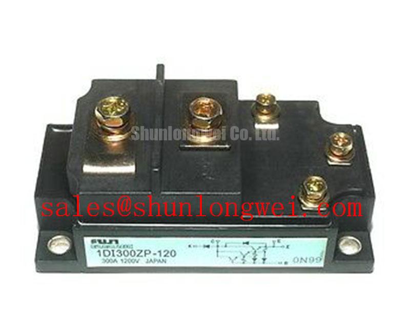
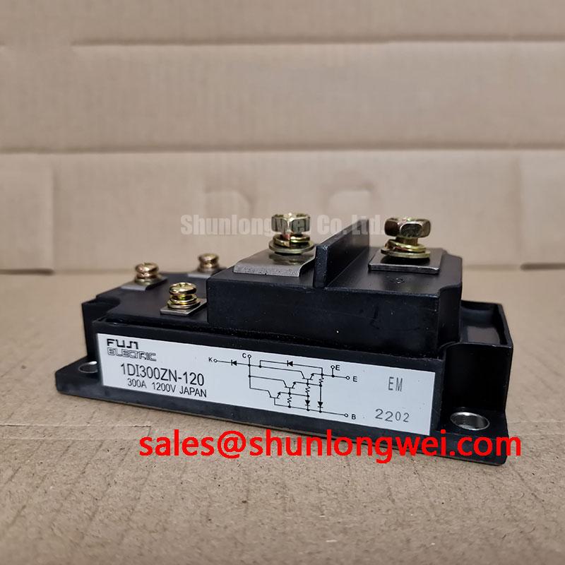
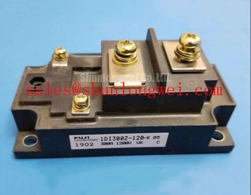
The Fuji Electric 1DI300ZP-120-05 is specified as a 1200.0 V, 300.0 A Power Transistor Module. These official ratings establish the module identity and are not a complete converter operating prescription. In a heavy duty variable frequency AC motor drive, the system engineer should validate the actual DC link voltage, switching overshoot, cooling condition, and fault response against the original drive documentation.
At elevated installation sites, terrestrial neutron exposure and single event burnout behavior require a system level review rather than an assumed module lifetime estimate. No FIT rate, altitude limit, cosmic ray withstand figure, or single event burnout performance value is stated here for this model. Design Consideration: where drives operate at high elevation, engineers should assess DC link headroom, transient voltage capture, protective coordination, and site conditions using the drive manufacturer’s qualification data and the applicable reliability plan.
Voltage derating is meaningful only when it is tied to measured switching waveforms. Probe the module terminals with an appropriately rated differential measurement method during representative acceleration, steady load, regenerative events, and commanded shutdown. A waveform that approaches the available voltage boundary may reflect layout inductance, insufficient clamping, cable reflection, or an abnormal commutation condition. The corrective action should be selected after the source of the transient has been isolated.
For general background on power module technologies and product families, see Fuji Electric Power Semiconductor and IPM Modules. This reference does not replace the original equipment circuit documentation for the installed drive.
1DI300ZP-120-05 Operational Boundaries: Evaluating Suppression of DC Link Voltage Doubling at Limits
Long motor leads can create reflected wave effects between the inverter output and the motor terminals. Under certain impedance and cable length conditions, reflected voltage can substantially increase the stress observed at the motor end and influence switching behavior at the converter. It is not appropriate to assume a fixed multiplier for every installation. Measure both the inverter output and the motor terminal waveform when cable related stress is suspected.
Engineering Recommendation: minimize the commutation loop area around the DC link, module terminals, and local capacitor connection to reduce inductive overshoot during switching. If field measurements show excessive ringing or a cable related waveform issue, the system integrator should evaluate output reactors, dv/dt filters, sine wave filters, or snubber arrangements according to the drive topology, motor cable characteristics, and measured peak margins.
Reverse recovery behavior from the associated freewheeling path can also affect ringing, conducted disturbance, and radiated emissions. The original converter design should be preserved unless qualified measurements support a change. A replacement module should not be treated as a standalone declaration of system EMC compliance. If a control board or power stack is under evaluation, the related Fuji Electric PIM seven pack information offers useful family context, while the installed circuit remains the governing reference.
⚠️ Maintenance Note: Periodically monitor terminal contact temperature rise and verify that heatsink airflow paths remain clear of dust accumulation.
Preventing Spurious Faults: Dynamic Braking Chopper Operation Guidelines for 1DI300ZP-120-05
During rapid deceleration, the motor returns kinetic energy to the DC link. The braking chopper, braking resistor, control threshold, and protective logic determine whether that energy is dissipated safely or whether an overvoltage response is triggered. The official information provided for the 1DI300ZP-120-05 confirms its voltage and current ratings but does not define an internal braking function, braking transistor arrangement, resistor value, or energy capability.
When investigating repeated DC link faults during deceleration, first compare the event timing with the speed command, load inertia, brake command, and resistor temperature condition. Check the braking resistor connections, thermal protection path, control feedback, and chopper gate command against the known drive schematic. A recurring trip can arise from several interacting conditions, including braking circuit operation, supply regeneration limits, a loose connection, or altered control timing.
The braking resistor and any external chopper device must be evaluated at system level for pulse energy, repetitive duty, enclosure heat removal, and fault containment. Avoid transferring values from another drive frame solely because its nominal current rating appears similar. For a related module family comparison during repair evaluation, review the published identity and ratings of 6MBI300U-120 alongside the original converter circuit, terminal arrangement, and control architecture.
Field Diagnostics & Commissioning: Dynamic Gate Impedance Control for Robust 1DI300ZP-120-05 Topologies
Before energizing a repaired power stage, confirm isolation from the mains supply, discharge the DC link using the approved equipment procedure, and inspect the gate drive board, gate return path, protection feedback wiring, and module terminal hardware. The supplied official parameters do not state gate threshold, gate charge, permissible gate voltage, internal topology, or an approved gate resistor value. Those details must be verified from the original equipment documentation and the applicable Fuji Electric datasheet.
Spurious turn on or cross conduction can be influenced by high switching dv/dt, shared return inductance, unsuitable gate impedance, degraded driver components, or a weak clamp path. Where the original topology uses active Miller clamping or negative gate bias, retain the manufacturer’s intended driver arrangement and validate it with isolated waveform measurements. Do not introduce a numerical gate bias or resistor setting without confirming compatibility with the gate driver, protection threshold, switching losses, and measured voltage stress.
During commissioning, begin with controlled conditions permitted by the equipment procedure and inspect collector or power terminal voltage, gate command behavior, current feedback, and fault response before returning the drive to production duty. Clean heatsink fins, check thermal interface condition, and recheck terminal fastening during scheduled maintenance because mechanical contact degradation can alter thermal performance over time. For gate loop measurement principles and switching test planning, consult Precision Gate Drive Design.