Content last revised on October 31, 2026
Preventing Spurious Faults: Damping Tail Current Oscillations in BSM150GB60DLC
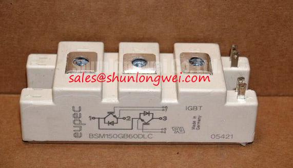
I separate the diode commutation event from the IGBT turn-off tail before changing gate resistance on a BSM150GB60DLC. With the equipment isolated and stored energy discharged, comparative resistance checks can reveal gross differences between switching paths, but they cannot establish switching performance. During controlled powered testing, correlate collector current, collector-emitter voltage and gate-emitter voltage with the protection signal. A fault coinciding with commutation deserves waveform investigation rather than an immediate protection-threshold increase.
Design Consideration: Antiparallel diode reverse recovery can add current to the incoming switch during turn-on. The peak reverse recovery current, I_rrm, and the abruptness of recovery affect overshoot and ringing; neither should be inferred from the module’s continuous current rating. Distinguish that event from the outgoing IGBT’s tail current by checking its position relative to the gate commands. Use suitably rated differential voltage and current probes, with measurement connections arranged to avoid introducing misleading ringing.
Gate resistance adjustment is an Engineering Recommendation for controlled evaluation, not a fixed repair prescription. Increasing turn-on resistance can reduce commutation severity while increasing switching loss. Compare the resulting gate waveform, collector-voltage peak and thermal behavior under the same operating conditions. An RC snubber should likewise be evaluated against the measured oscillation and its own dissipation; installing an arbitrary capacitor across the switching path can simply move stress elsewhere.
Inspect the external commutation loop before attributing every oscillation to the semiconductor. Closely coupled outgoing and return conductors can reduce parasitic inductance, provided the assembly preserves the equipment’s required electrical clearances. Keep snubber connections local to the relevant current loop. Infineon’s OptiMOS™ and CoolMOS™ Power MOSFET portfolio concerns different device technologies; its voltage classes and switching characteristics must not be substituted for this IGBT module’s limits.
Benchtop Waveform Tuning: Derating and Parameter Mismatch in BSM150GB60DLC
Compare gate timing and current distribution under repeatable thermal conditions before deciding that parallel modules are electrically matched. The supplied Official Specifications identify 150 A at case temperature 80°C, typical collector-emitter saturation voltage of 1.95 V, and total power dissipation of 700 W at case temperature 25°C. The typical saturation voltage is not a guaranteed value throughout the operating range, and the dissipation rating is not a permissible continuous equipment heat load independent of cooling.
Design Consideration: Where the device characteristic curves show a positive temperature coefficient of saturation voltage at the operating current, that behavior can assist static current sharing. It does not establish dynamic balance. Symmetrical gate-loop routing, comparable emitter-return impedance and consistent thermal interfaces remain important when assessing paralleled switching positions. Compare each branch during turn-on and turn-off rather than relying solely on steady-state current readings.
Review the controller’s conduction pattern alongside the DC-link waveform. Phase-angle-controlled equipment can produce discontinuous charging and line-frequency ripple that changes instantaneous switching stress. In PWM equipment, do not treat phase-angle adjustment as a general tuning method: preserve the intended modulation strategy and investigate the actual source of bus ripple. Evaluate capacitor condition and connections before attempting to conceal a supply-side problem with gate damping or an RC snubber.
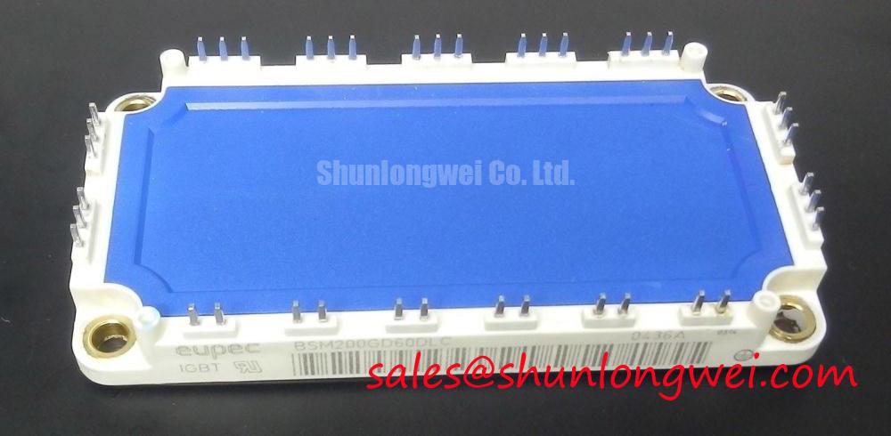
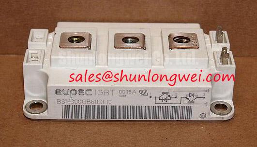
For replacement assessment, BSM200GB60DLC is a related model worth comparing, not an automatic substitute. Check its terminal arrangement, outline, gate-drive requirements, switching characteristics and cooling requirements against the original assembly. A different current designation does not establish compatibility. Infineon’s CIPOS™ Nano IPM series represents a separate integrated product family, so its drive and protection arrangements should not be assumed for this module.
For a utility-scale 1500 V central solar photovoltaic inverter, evaluation of this 600 V device requires a topology that constrains each device’s blocking stress; it cannot be connected directly across that DC bus. The system-level discussion in Peak Efficiency in Solar and Energy Storage provides context for multilevel architectures, not evidence of this module’s suitability or service life in a particular inverter.
BSM150GB60DLC Circuit Protection & Reliability: Calibrating Overcurrent Protection within SCSOA Limits
Measure the complete fault-clearing sequence from fault onset through current suppression, rather than timing only the comparator output. The supplied Official Specification gives a short-circuit withstand time of 10 µs. Treat that as a conditional device limit, not an allowable detection delay: sensing, blanking, propagation and turn-off all consume the protection interval. Short-circuit safe operating area assessment must include the applicable bus voltage, gate conditions and initial junction temperature.
Design Consideration: A type-I event starts with turn-on into an existing short circuit; a type-II event develops while the device is already conducting. Their current and desaturation waveforms differ, so protection evaluation should address both situations using a suitably controlled test arrangement. Begin protection-chain checks with simulated fault signals where practical, establishing controller inhibition and driver response before conducting hazardous power-stage fault tests.
Two-stage soft turn-off is an Engineering Recommendation to evaluate when abrupt fault interruption produces excessive collector-emitter overshoot. The driver initially controls current reduction, then completes turn-off. Its effectiveness depends on driver behavior, gate impedance and the external power loop. An excessively slow response can increase fault energy, while an excessively abrupt response can increase inductive overvoltage; verify both current decay and voltage stress together.
Check laminated busbar alignment and the local DC-link connection during that assessment. Minimize the commutation-loop area without compromising required clearance, and evaluate voltage peaks at the module terminals. Where long motor cables are present, reflected-wave stress at the motor is a separate transmission-line issue: cable length, edge rate and termination determine whether an output reactor or filter merits evaluation. Module-terminal measurements alone do not characterize motor-terminal stress.
Semiconductor fuse coordination also remains a system exercise. Compare the fuse’s clearing behavior and I²t information with the converter’s prospective fault current and documented withstand limits. A fuse can contribute to branch fault isolation, but its presence does not replace fast gate-driver protection or establish that the IGBT survives a short circuit.
Field Diagnostics & Commissioning: Preventing Terminal Stress in BSM150GB60DLC Assemblies
Check screw engagement against the terminal drawing before applying final tightening torque. A screw can bottom out without clamping the conductor, while insufficient engagement can leave an unreliable joint. Assess the complete stack of conductor, washer and fastener against the specified hardware arrangement. Do not infer screw length or tightening torque from the module’s current rating.
Design Consideration: Support the external busbar so its weight and thermal movement do not lever against the module terminals. Bring conductors into alignment before tightening rather than using the terminal screws to pull a displaced busbar into position. Inspect contact faces, mounting flatness and evidence of uneven seating. Mechanical loading at an external terminal can affect the assembly without establishing any particular internal construction or failure mechanism.
Field Alert: Never use terminal tightening force to pull a misaligned busbar into place; align and support the conductor before applying the specified fastening procedure.
During commissioning, compare joint temperature rise and voltage drop under controlled loading, using methods suitable for the energized equipment. An unusual hot spot can justify checking contact condition, clamping and current distribution, but it does not identify a single cause. Record the installed hardware and torque procedure so later maintenance can distinguish an assembly change from an electrical change. Complete the assessment with secure conductor support, unobstructed cooling and strain-free gate connections.