Content last revised on October 18, 2026
Assembly Integrity & Layout Architecture: Implementing Gate Driver Auxiliary Power Sequencing for CM150RX-24T/300G
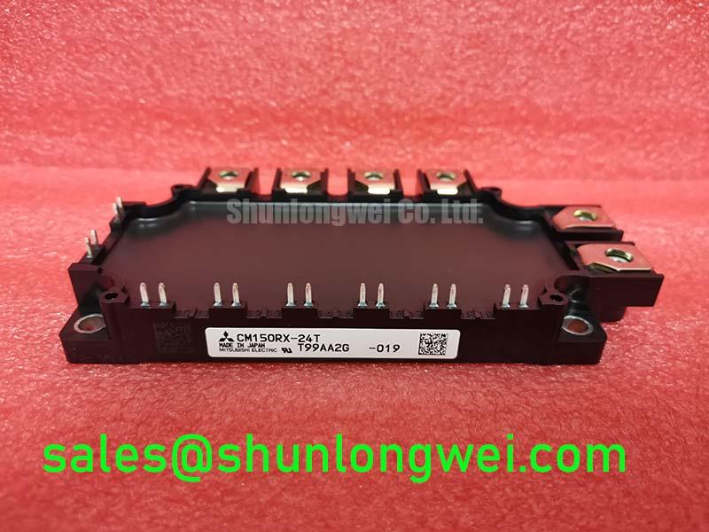
Isolate the DC link, discharge the bus, and verify the gate driver auxiliary rails before probing the CM150RX-24T/300G in a heavy duty variable frequency AC motor drive. The module is identified by the supplied official product data as a Mitsubishi Electric IGBT module rated at 1200.0 V and 150.0 A, with a module package. These ratings define the component identity; the permitted switching conditions, thermal limits, gate requirements, and protection thresholds remain system-level design matters.
During a replacement assessment, record the original gate-driver connections, DC-link polarity, phase-leg position, and braking-chopper topology before removing the installed device. A high-voltage drive may contain both motor inverter legs and a regenerative braking path connected to a large braking resistor. The replacement process therefore requires more than matching voltage and current markings. The engineer must confirm the original electrical topology, cooling interface, auxiliary power sequence, and protection coordination.
Establish the gate-driver auxiliary supply and undervoltage lockout sequence before applying the high-voltage DC link. A practical integration sequence is to power the isolated driver control side, confirm that the driver reports a stable ready state, verify the intended turn-off bias, and only then permit the DC-link contactor or precharge sequence to proceed. The negative turn-off bias range of −5 V to −15 V should be treated as an engineering design target for the driver circuit described in the installation brief, not as an official standalone rating of the IGBT module.
The driver supply return must follow the intended emitter reference for each switching position. Do not assume that a control-board ground is interchangeable with the power-emitter reference. In a half-bridge or braking-chopper assembly, a misplaced return path can add common-source inductance and distort the actual gate-to-emitter voltage seen during rapid switching. The system integrator should map every auxiliary terminal from the original drive documentation and confirm polarity with the power stage fully isolated.
Layout work should keep the gate loop compact and separated from the high-current commutation path. Gate and emitter conductors should be routed as a controlled pair, while the DC-link and braking-current paths should use short, symmetrical connections suited to the mechanical construction of the drive. Clearance around high-voltage copper, mounting hardware, and insulated busbar supports must be assessed against the applicable equipment insulation rules and the enclosure environment. The module’s 1200.0 V rating does not itself certify the complete assembly for any particular working voltage or pollution condition.
In regenerative braking service, the gate driver must coordinate the braking transistor with the DC-link sensing and resistor network. A braking command that arrives while the driver is in an undervoltage or reset state can leave the switching device unavailable, while an incorrectly sequenced command can produce uncontrolled current in the braking branch. Confirm that the controller inhibits the high-voltage enable signal whenever the driver supply is outside its validated operating window. Use an isolated probe to observe the gate-to-emitter waveform during controlled commissioning, with the DC-link initially limited by the equipment’s approved test procedure.
The fast fuse protecting a braking branch should be assessed with the semiconductor’s short-circuit behavior and the fuse’s clearing characteristics as a coordinated system. Compare the fuse let-through I²t with the protection study for the drive rather than selecting a fuse from the module current number alone. A fuse that interrupts too slowly can expose the semiconductor to destructive energy, while an unsuitable fast fuse can create nuisance interruptions during normal regenerative pulses. The final choice belongs to the drive protection design and must be validated against the actual DC-link and braking-resistor conditions.
For field troubleshooting, inspect the auxiliary supply under both idle and enable commands, then compare the driver status signal with the contactor sequence. A gate waveform that collapses during a braking event may point to supply impedance, isolation behavior, UVLO interaction, or a layout-related transient. Correlate the waveform with DC-link voltage, phase current, and the controller’s fault timestamp instead of assigning the symptom to the module alone.
Preventing Spurious Faults: Active Miller Clamp Implementation Guidelines for CM150RX-24T/300G
Use a dedicated active Miller clamp architecture when the switching node can couple transient voltage into the opposite device gate. The clamp should be located close to the driver output and the relevant gate-emitter loop so that the clamp path does not share unnecessary inductance with the turn-on path. The suggested negative gate-bias range of −5 V to −15 V is a design consideration for suppressing unintended turn-on; the driver manufacturer’s voltage limits and the complete gate-emitter insulation requirements must govern the final circuit.
Terminal identification deserves particular care during a replacement. Confirm the power terminals, gate connection, emitter reference, and any auxiliary emitter or sense connection from the correct mechanical drawing before tightening busbars or applying a pulse. The supplied product data identifies the package as a module but does not establish a universal terminal arrangement. That arrangement must be matched to the actual Mitsubishi Electric documentation and the drive’s original conductor layout.
High dv/dt at the switching node can create a transient gate-emitter voltage through the coupling capacitance of the complementary device and the stray inductance of the gate loop. An active Miller clamp provides a low-impedance path during the off state, but it cannot compensate for an incorrectly referenced emitter, excessive loop inductance, unstable isolated power, or poor driver timing. Check the clamp activation timing against the driver’s own logic behavior and ensure that the clamp does not fight a commanded turn-on pulse during the dead-time transition.
Dead-time coordination is especially important in an inverter leg and in a regenerative braking chopper sharing a DC link. The controller should prevent simultaneous commands to opposing switches, while the driver must maintain a defined off state during reset, UVLO, and auxiliary supply startup. Verify the gate signals at the module terminals rather than only at the driver-board connector. A clean signal at the board can still become distorted after passing through a long harness, connector, or mechanically flexible busbar assembly.
Inspect creepage and clearance around the gate-driver isolation boundary, power terminals, and floating phase nodes. Contamination, condensation, vibration, and cable movement can change the effective electrical environment inside a drive cabinet. Mechanical fastening also matters: a busbar that shifts under vibration can alter contact resistance and introduce intermittent switching behavior. Use the equipment manufacturer’s fastening procedure and recheck the conductor alignment after the module is seated.
When evaluating a possible cross-reference, the CM450DX-24S1 should be treated as a separate device requiring its own voltage, current, package, terminal, gate-drive, and thermal verification. The following comparison keeps the supplied identification data distinct from system assumptions.
| Device | Official voltage data supplied | Official current data supplied | Package data supplied | Replacement review |
|---|---|---|---|---|
| CM150RX-24T/300G | 1200.0 V | 150.0 A | Module | Confirm terminal arrangement, gate requirements, cooling interface, and protection coordination |
| CM450DX-24S1 | Verify from its product documentation | Verify from its product documentation | Verify from its product documentation | Do not treat the part number as a drop-in equivalence without electrical and mechanical validation |
For the switching-node investigation, use a properly rated differential probe and observe the gate-emitter voltage of both the commanded and opposing devices. Compare the turn-off waveform, clamp action, and DC-link transient under controlled current conditions. The Mitsubishi Electric Power Semiconductors & High-Power Modules resource provides the relevant manufacturer technology context, while the Mitsubishi Electric Global Semiconductor Device Technologies site should be used for manufacturer-level device information.
🔧 Pro Tip: Keep the gate-driver return and power-emitter reference physically controlled, then verify the actual gate-emitter waveform at the module during a limited-energy switching test rather than relying on the driver-board measurement point.
Benchtop Waveform Tuning: Mitigating Stress via Thermal Paste Degradation Prevention and Mounting Control for CM150RX-24T/300G
Prepare the heatsink interface before waveform tuning because thermal contact quality affects the electrical test window. Remove residue from the heatsink and module mounting surface, inspect the baseplate seating area, and apply a uniform thermal interface layer appropriate to the selected material and mounting procedure. Excess material can increase thermal resistance, while incomplete coverage can leave local hot regions beneath the baseplate.
Baseplate curvature and heatsink flatness should be considered together. A rigid mounting surface can force contact at limited points if the mating surfaces are contaminated, distorted, or unevenly loaded. Use the mounting pattern specified for the mechanical assembly and tighten the fasteners progressively so the module seats without twisting. A sequential cross-pattern is a common design consideration for distributing pressure, but the manufacturer’s mechanical instructions and the drive builder’s approved torque procedure take priority.
Thermal paste degradation is often associated with long-term thermal cycling, pump-out, contamination, or excessive mechanical movement. During service inspection, look for dry regions, displaced compound, or evidence that the baseplate has not remained evenly supported. Do not infer semiconductor damage from paste appearance alone. Correlate the thermal interface condition with temperature measurements, switching duty, cooling airflow, and the drive’s fault history.
The benchtop waveform should be interpreted alongside the thermal response. A turn-off overshoot can reflect commutation-loop inductance, while a temperature rise can involve interface resistance, cooling performance, switching frequency, current profile, or braking-resistor duty. Minimize the power commutation loop and keep the gate loop independent, then verify peak voltage and current margins against the DC-link conditions during controlled switching tests. The Power Electronics Masterclass offers additional system-level context for IGBT selection and switching reliability.
For the braking path, tune the pulse sequence with attention to the energy absorbed by the resistor and the recovery behavior of any associated diode. A bootstrap supply, where used by the driver architecture, also requires sufficient high-frequency charge transfer and suitable diode recovery behavior; these are properties of the selected driver and auxiliary circuit, not confirmed characteristics of the IGBT module itself. Confirm the driver supply under the actual pulse pattern rather than under static current only.
After assembly, perform a low-energy functional check, confirm the gate-off state during controller reset, and inspect the thermal interface after the first controlled operating interval. When the module is installed in a heavy-duty variable frequency AC motor drive, the final acceptance decision should combine the official 1200.0 V voltage rating, 150.0 A current rating, correct module mechanics, gate-driver behavior, fuse coordination, braking-resistor duty, and measured thermal performance.