
Content last revised on October 26, 2026
Benchtop Waveform Tuning: Mitigating Stress via Cosmic Ray Robustness and Voltage Derating on CM400DY-66H
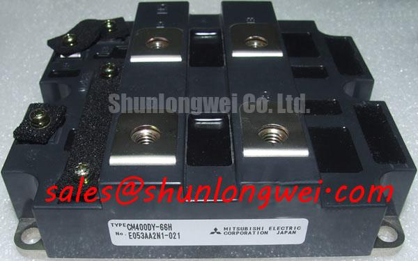
Manufacturer: Mitsubishi Electric | Model: CM400DY-66H | Category: IGBT Module | VCES: 3300 V | IC: 400 A at TC = 25°C
Before applying a high-voltage DC link, I check the switching bench for excessive collector-emitter overshoot, probe reference errors, and unintended current paths around the module terminals. The CM400DY-66H carries an official collector-emitter voltage rating of 3300 V, but that rating does not replace a system-level transient review. The measured switching waveform must remain within the voltage and current boundaries established for the complete converter, including stray inductance, commutation behavior, gate timing, and protection response.
Cosmic-ray and terrestrial-neutron effects are high-risk reliability topics, particularly when equipment operates at elevated altitude. A credible Single Event Burnout assessment requires device-specific test evidence, mission profile data, neutron spectrum assumptions, voltage distribution, switching state, and an accepted reliability model. The available product parameters alone do not establish a FIT value or a guaranteed altitude limit for this module. For a wind converter installed above approximately two thousand metres, treat altitude-related SEB exposure as a design investigation rather than assigning a universal derating percentage.
On the bench, use a properly rated differential voltage probe and place the measurement reference as close as practical to the module power terminals. Capture turn-off voltage, current commutation, gate-emitter voltage, and the timing of the protection circuit in the same record. A high apparent spike can result from probe-loop inductance or an unsuitable measurement reference, while a genuine overshoot generally follows the switching current path and changes with bus voltage, gate resistance, load current, or commutation layout.
The principal layout action is to minimize the power commutation loop and keep the gate-drive return separate from the high-current emitter path until the intended connection point. Laminated or closely coupled busbar construction can reduce parasitic loop inductance, but the final arrangement remains system-dependent. During validation, the engineering team should compare peak voltage against the DC-link operating envelope under cold, hot, light-load, and high-current switching conditions. A single room-temperature waveform is not sufficient evidence for a high-energy converter.
For repair evaluation, compare the installed module identification, terminal arrangement, gate-drive polarity, cooling interface, and protection thresholds with the original converter documentation. The CM400DY-66H is rated for 800 A peak collector current in pulse operation, while its listed continuous DC collector current is 400 A at TC = 25°C. These are different ratings and should not be merged when reviewing a wind turbine full-scale converter or its machine-side and grid-side switching bridges.
CM400DY-66H Circuit Protection and Reliability: Calibrating Driver Power Stage Start-Up Inrush Mitigation
Gate-driver auxiliary power must reach a stable operating condition before the converter applies high-voltage DC-link power. The driver supply sequence should establish the intended gate-off state, confirm undervoltage lockout operation, and block switching commands during auxiliary-power start-up. A negative turn-off bias may be evaluated by the system designer, commonly within the driver manufacturer’s validated operating range, but it is not an official electrical characteristic stated for the CM400DY-66H.
The practical objective is to prevent a partially powered driver from allowing the gate-emitter voltage to drift through the Miller region. The driver supply monitor, desaturation or overcurrent protection, interlock logic, and gate clamp should be checked as a coordinated chain. Use an oscilloscope to confirm that the gate remains in its defined off state while the DC link rises. If the gate waveform moves before the driver reports a valid supply, inspect the auxiliary supply ramp, isolation barrier behavior, pull-down path, and controller reset timing.
Gate-drive source and sink capability should be selected from the required gate-charge profile, switching frequency, desired transition time, and the total impedance of the driver loop. The CM400DY-66H parameters discussed here do not establish a mandatory external gate resistor. Therefore, the external resistor is a tuning component, not a fixed replacement value. A smaller value can accelerate transitions while increasing ringing and electromagnetic stress; a larger value can reduce ringing while increasing switching loss. Select and verify it through measured gate and collector waveforms.
Use separate turn-on and turn-off impedance only when the driver topology and protection strategy support that arrangement. The resistor must be placed close to the gate terminal, with a compact return path to the corresponding emitter connection. Long flying leads can make a correctly selected resistor appear ineffective because the added inductance becomes part of the gate circuit. During fault testing, confirm that the protection circuit actively removes gate drive and does not depend solely on the controller software to stop the pulse train.
⚠️ Field Alert: Isolate auxiliary and high-voltage supplies and verify that the DC link and other stored-energy circuits are safely discharged before disconnecting gate-drive wiring. Follow the original assembly procedure for terminal pressure, thermal compound, and mechanical fastening.
For a broader component assessment, the UM100CDY-10 may be reviewed separately, but its electrical role and ratings must be evaluated independently. Its inclusion here does not establish suitability for the same converter or compatibility with the CM400DY-66H switching position.
Transient Dynamics and Electrical Design: Dynamic Gate Impedance Control for Robust Operation on CM400DY-66H
High dv/dt at the collector can couple through the effective Miller capacitance and disturb the gate-emitter voltage of an otherwise inactive device. The risk is cross-conduction, false turn-on, or a gate waveform that rings through the driver’s protection threshold. The correct response is to control the complete gate loop, not to assume that a nominal driver voltage alone will suppress the disturbance.
A low-impedance active Miller clamp can hold the inactive gate near its defined off potential when the complementary switch changes state. Its effectiveness depends on clamp placement, driver current capability, emitter-reference integrity, isolation behavior, and the timing relationship between the main gate path and the clamp path. When a negative turn-off bias is used, the driver must be rated for that condition and the gate-emitter voltage must remain within the module’s permitted operating limits.
Inspect the gate waveform directly at the module terminals, not only at the driver output connector. Compare the active and inactive channels during complementary switching. A disturbance that appears only at the module may indicate gate-loop inductance, shared emitter impedance, capacitive coupling from the power bus, or an unsuitable probe connection. A disturbance already visible at the driver output points toward the driver supply, command timing, isolation barrier, or local decoupling.
The power bus and gate circuit should be routed so that high di/dt current does not share the gate-return conductor. Keep the driver physically close to the module and maintain the required creepage and clearance for the converter’s working voltage and pollution environment. These distances are system design requirements determined by insulation coordination, enclosure conditions, and the applicable equipment standard; they are not special CM400DY-66H datasheet ratings.
During commissioning, test dead time and interlock behavior at the actual operating temperature and load range. Check whether the inactive gate remains stable when the opposing device turns on, then inspect the collector-emitter waveform for signs of simultaneous conduction. The official VGE(th) range is 4.5 to 7.5 V at IC = 40 mA and VCE = 10 V. This threshold test condition should not be treated as a normal switching gate-drive target; it is a device characterization condition.
Field Diagnostics and Commissioning: Antiparallel Freewheeling Diode Reverse Recovery in CM400DY-66H Topologies
When the antiparallel diode commutates, reverse-recovery current can interact with bus inductance, the opposing IGBT, and the gate-drive timing. The resulting current peak and di/dt may produce voltage overshoot, ringing, and unwanted electromagnetic emissions. The CM400DY-66H lists a diode forward voltage of 3.30 V typical at IE = 400 A, but the supplied parameters do not define a universal reverse-recovery current or recovery-time value for every operating condition.
Measure diode commutation with synchronized voltage and current probes. Record the load current, junction or case temperature, DC-link voltage, turn-on gate resistance, and physical bus arrangement for each test point. A sharp current transition can be associated with diode recovery, layout inductance, probe bandwidth, or a combination of these effects. Compare the waveform with the known-good converter channel rather than assigning a fault from one voltage reading.
An RC snubber can be considered when measured ringing exceeds the system’s transient or emissions objectives. Its capacitance, resistance, pulse-energy capability, and physical placement must be selected from the measured ringing frequency and loss calculation. The snubber should sit across the relevant commutation path with the shortest practical connection. An oversized capacitor can increase switching loss and device current, while an unsuitable resistor may add little damping.
Turn-on gate resistance is another tuning variable. Increasing it can reduce the aggressiveness of the opposing device’s turn-on and may lower recovery-related overshoot, but the resulting switching loss and thermal load must be checked. The VCE(sat) specification is 4.40 V typical at IC = 400 A and VGE = 15 V; it provides a reference for conduction characterization under the stated test condition, not a complete prediction of converter loss during dynamic commutation.
The thermal path also requires disciplined inspection. The listed IGBT thermal resistance is 0.036 °C/W per half module, while the diode thermal resistance is 0.072 °C/W per half module. These values should be used with the correct loss split and cooling model. Verify flatness, interface coverage, clamping uniformity, and the original mechanical arrangement before attributing a high-case-temperature alarm to the semiconductor itself.
For comparative system research, engineers can review CM1500HC-66R as a separate Mitsubishi Electric module reference, while the manufacturer’s High-Voltage HVIGBT Modules and NX-Series IGBT Modules pages provide broader product-family context. The Industrial Applications resource may also assist engineers reviewing high-power converter architectures, while final compatibility remains dependent on the original topology, gate driver, cooling assembly, and protection settings.