Content last revised on October 15, 2026
FF200R17KE3 Operational Boundaries: Pre-Installation Health Check
Remove DC link power, discharge the assembly, and use a grounded ESD workstation before checking the cold-state terminals of the FF200R17KE3. In diode-test mode, compare the main semiconductor paths and antiparallel diode path with the known-good phase position, then inspect gate-to-emitter leakage without applying external drive voltage. This incoming inspection establishes a practical baseline before the module is installed in a high-energy converter.
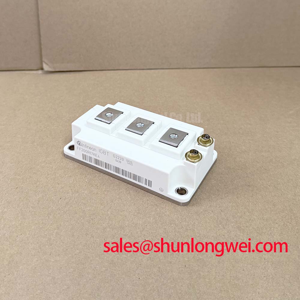
The FF200R17KE3 is an Infineon IGBT module rated at 1700.0 V and 200.0 A, with a Module package designation. These are official product parameters supplied for product identification. The rating does not replace a system-level review of switching conditions, cooling, protection coordination, or the original equipment manufacturer’s mechanical interface.
Cold unpowered screening should begin with a visual check of the housing, power terminals, control terminals, mounting surface, and insulating interfaces. Look for cracked plastic, displaced terminal hardware, contamination, or marks that could affect creepage and clearance. The inspection should be performed with the module isolated from gate-driver circuitry and with all capacitors in the test fixture safely discharged.
Use the digital multimeter diode function to check the expected semiconductor conduction paths between the main terminals and the antiparallel diode path. Record polarity, displayed forward indication, and any open-circuit indication rather than treating one meter reading as a complete health certificate. A result that differs materially from the matching phase position may justify a second measurement with reversed leads, followed by comparison against an unused or known-good module from the same equipment family.
The gate terminals require a separate low-energy check. Confirm gate-to-emitter isolation with the meter in an appropriate resistance or continuity mode, keeping the test current limited by the instrument. Do not charge the gate with an external supply during incoming inspection. Unstable readings, unexpected continuity, or a changed result after handling should trigger ESD-controlled remeasurement and review of the test leads before the part is accepted.
For a utility-scale 1500V high-power central solar photovoltaic inverter, the installation team should also audit the physical spacing around the power terminals and gate-driver wiring. Keep high-voltage conductors separated from low-level control paths, maintain the original insulation barriers, and route the gate loop as a compact forward-and-return circuit. The system designer remains responsible for validating clearances against the applicable equipment insulation design and installation environment.
Bench Tip: Keep the module, meter leads, and test fixture at the same cold-state reference condition, and use ESD protection while comparing the gate leakage and diode readings.
Transient Dynamics & Electrical Design: Torque Reaction Absorption and Terminal Stress Prevention on FF200R17KE3
Power-terminal hardware should be installed without side loading the module body. Check that the screw enters the intended thread cleanly, that the washer bears evenly, and that the busbar does not lever against the terminal during tightening. A misaligned copper bar can transfer vibration and thermal-cycle stress into internal electrical joins even when the external terminal appears secure.
Use a calibrated torque tool and follow the equipment or module assembly documentation for the approved fastener, washer arrangement, and tightening sequence. The torque value is an installation requirement, not an electrical rating of the IGBT. After tightening, verify that the busbar remains flat and that no terminal rotates when the connected conductor is gently checked with the power isolated.
Protection coordination must be reviewed at the converter level. A high-speed semiconductor fuse should be selected by comparing its clearing behavior and I2t characteristic with the module’s fault withstand and surge data from the applicable technical documentation. The analysis should include prospective short-circuit current, DC-link energy, fuse tolerance, commutation path inductance, and the response delay of the gate driver. A fuse that clears quickly in isolation may still be poorly coordinated if the driver, bus structure, and fault loop allow excessive current before interruption.
For replacement work, the FF900R17ME7_B11 can be reviewed as a related device in the same high-power IGBT product family. It should not be treated as an automatic substitute: voltage class, current definition, circuit topology, terminal geometry, gate characteristics, thermal interface, and protection settings all require a documented compatibility check.
| Device | Product category | Published voltage | Published current | Replacement review |
|---|---|---|---|---|
| FF200R17KE3 | Infineon IGBT Module | 1700.0 V | 200.0 A | Reference device for installation and test comparison |
| FF900R17ME7_B11 | Related IGBT module | Consult applicable product documentation | Consult applicable product documentation | Evaluate only after electrical and mechanical matching |
During commissioning, capture switching-node behavior with suitable high-voltage differential measurement and current measurement. Examine turn-off overshoot, ringing, diode recovery interaction, gate plateau behavior, and the effect of dead time. Minimize parasitic inductance in the power and gate loops, then verify peak voltage and current margins under the actual DC-link and load conditions. The driver’s gate resistor, damping network, active clamp, and dead-time settings are system-dependent values rather than fixed FF200R17KE3 product parameters.
FF200R17KE3 Circuit Protection & Reliability: Calibrating Floating Gate Bias Supply Decoupling
The floating gate-driver supply must reach its intended operating state before the high-voltage DC link is enabled. A practical sequence is to validate auxiliary supply startup, gate-driver UVLO status, desaturation or fault interlock behavior, and the turn-off bias at the driver output under no-load conditions. The requested negative turn-off bias range of −5 V to −15 V should be treated as a system integration target requiring confirmation against the selected driver, isolation scheme, and applicable module documentation, not as an official FF200R17KE3 rating.
Place the local driver decoupling network close to the driver supply pins and keep its charging and return paths separate from high-current emitter switching paths. The bootstrap capacitor, where used by the chosen driver topology, must retain sufficient charge during the intended high-side on-time. Its charging path should be checked for diode recovery effects, series resistance, leakage, switching frequency, and driver quiescent demand. A bootstrap arrangement is not interchangeable with an isolated bias supply without rechecking startup, duty-cycle, UVLO, and fault-reset behavior.
Gate-loop parasitic inductance can convert rapid current changes into unwanted gate voltage movement. Keep the outgoing gate path and return path tightly coupled, avoid unnecessary connector length, and locate damping components according to the driver layout. During a controlled switching test, check whether ringing crosses the driver’s unintended turn-on region or disturbs the Miller plateau. Any active clamp or Miller clamp should be validated with the actual gate charge, collector voltage transition, and driver propagation delays.
When several modules or semiconductor positions operate in parallel, positive temperature coefficient behavior can assist static current sharing, but it does not remove the need to match gate-drive timing, wiring impedance, thermal conditions, and dynamic current paths. Use current probes and synchronized voltage measurements to compare turn-on and turn-off behavior across positions. The gate driver should provide a defined fault state before DC-link energization, with UVLO and interlock signals tested through the complete protection chain rather than only at the controller pins.
The Infineon IGBT Modules & Discretes Official Portfolio provides manufacturer-level product context, while the Infineon TRENCHSTOP™ IGBT3 application note offers relevant background on IGBT switching behavior. These references support design interpretation but do not replace the exact device-specific ratings and application conditions for this model.
Transient Dynamics & Electrical Design: Baseplate Convexity Inspection on FF200R17KE3
Before mounting the FF200R17KE3, inspect the module baseplate and heatsink contact area for burrs, contamination, local high spots, or visible distortion. The heatsink should be clean and sufficiently flat for the specified thermal interface method. A hard particle beneath the baseplate can create concentrated mechanical loading, while a surface mismatch can produce uneven thermal transfer across the module.
Apply the selected thermal interface material as a continuous, controlled layer suited to the equipment assembly process. A typical industry design consideration is a thin, uniform interface layer in the approximate 50 to 80 µm range, but the final value depends on the material, surface finish, application method, and manufacturer instructions. The installer should verify coverage without allowing excess compound to migrate into terminals or insulation barriers.
Use a diagonal cross-pattern when bringing the mounting hardware down, allowing the baseplate to settle progressively against the heatsink. The final torque must come from the applicable mechanical documentation for the module, fastener size, washer system, and heatsink. Do not infer the correct torque from the electrical current rating. Recheck that the module body is not being forced into alignment by the busbars or cable assembly.
After assembly, inspect the interface for displaced material and confirm that the power terminals remain mechanically neutral. Thermal validation should be performed under the intended switching profile, airflow, heatsink orientation, and enclosure conditions. Compare temperatures at equivalent phase positions and review thermal transients during startup, load changes, and shutdown rather than relying only on a single steady-state reading.
For the surrounding rectification and DC-link topology, engineers may also evaluate the related FF500R12KE4 as a separate complementary product reference. Its presence in a power-conversion chain does not establish electrical compatibility with the FF200R17KE3; voltage coordination, current path, switching role, insulation system, and mechanical integration must be assessed independently.
Long-duration validation should combine thermal cycling, insulation checks, gate-driver fault testing, and switching waveform review under controlled laboratory procedures. The Ultimate IGBT Knowledge Base can be used as broader technical reading on IGBT principles, physical behavior, and application analysis.