

Content last revised on September 10, 2026
FF400R12KT3 Thermal-Electrical Optimization: Kelvin Emitter Connection Practical Tuning
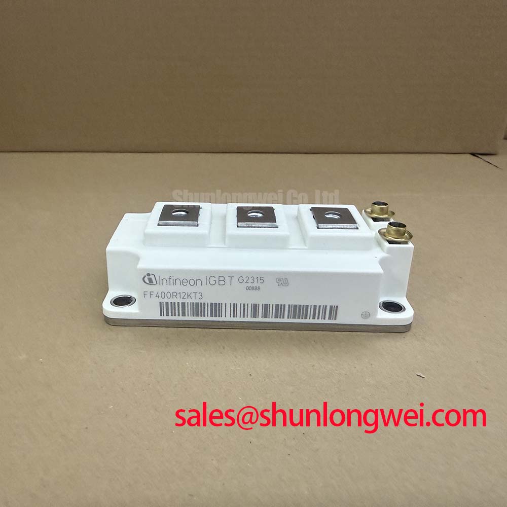
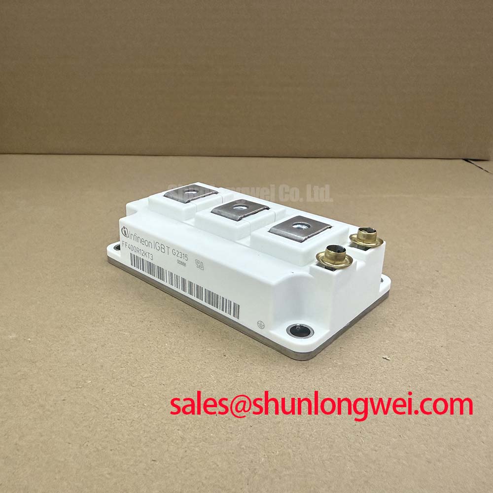
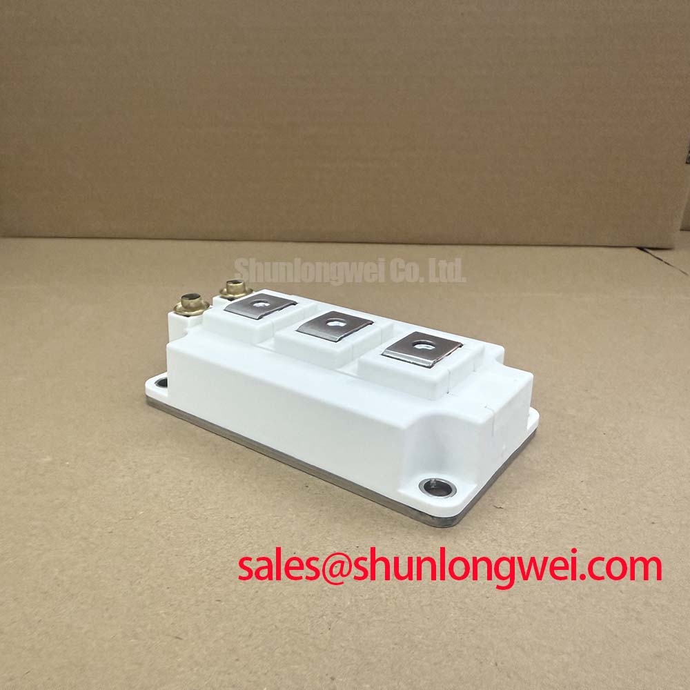
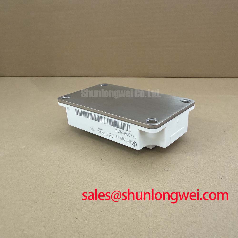
Check the nameplate against the approved replacement record, inspect the isolated baseplate and terminals, and confirm the electrical boundary before connecting an FF400R12KT3 module. The Infineon device is a 1200 V IGBT module with a 400 A continuous DC collector current rating under the stated datasheet condition. Its housing is a 62 mm C-Series package with an isolated baseplate and pre-applied phase-change thermal interface material.
| Parameter | Official Specification |
|---|---|
| Manufacturer | Infineon |
| Collector-emitter voltage | VCES = 1200 V at Tvj = 25°C |
| Continuous DC collector current | IC nom = 400 A at TH = 65°C and Tvj max = 150°C |
| Repetitive peak collector current | ICRM = 800 A for tp = 1 ms |
| Gate-emitter peak voltage | VGES = ±20 V |
| Collector-emitter saturation voltage | VCE(sat) = 1.70 V typ. at IC = 400 A, VGE = 15 V, Tvj = 25°C |
| Thermal interface material | Pre-applied phase-change material |
| Comparative tracking index | CTI > 400 |
| Package | 62 mm C-Series with isolated baseplate |
Before commissioning, measure the gate-emitter path with the power stage isolated and compare the result with the approved wiring diagram for the equipment. The module’s published electrical data does not establish a separate auxiliary or Kelvin-emitter pin definition, so the system integrator should verify the actual terminal assignment from the original Infineon documentation and the machine schematic. Do not infer a driver return connection from the physical position of a terminal alone.
Design Consideration: Where the qualified gate-drive topology provides a separate emitter-sense return, keep that low-current reference independent from the high-current emitter path for as much of the switching loop as the mechanical design allows. The purpose is to reduce common emitter inductance and prevent the driver from sensing voltage generated by load-current commutation. Main emitter conductors, gate-return conductors, and shield or chassis connections should follow the approved topology rather than being joined at several uncontrolled points.
During bench testing, monitor the gate-emitter voltage directly at the module terminals with a suitable differential probe. A ringing waveform, inconsistent turn-off level, or pulse that changes when the load busbar is moved may indicate parasitic coupling, probe-loop error, or an unsuitable return path. Compare the waveform with a known-good assembly and confirm that the measured peak remains inside the official ±20 V VGES boundary. Gate resistance, driver supply behavior, dead time, and cable routing remain system-determined values.
For equipment selection, engineers can place the FF400R12KT3 beside other 1200 V module candidates, including FZ800R12KS4_B2, but replacement approval requires a complete check of voltage, current, gate-drive interface, mechanical footprint, thermal path, and switching behavior. A similar voltage class alone does not establish electrical interchangeability.
Thermal inspection should begin at the mounting surface. Remove contamination from the heatsink, check for uneven contact marks, and confirm that the pre-applied phase-change material has not been damaged or displaced during handling. If the assembly uses a pressure plate, spring washers, or a two-sided cooling arrangement, the maintenance team should calibrate the clamping process against the equipment manufacturer’s mechanical specification rather than applying an assumed force.
Field Diagnostics & Commissioning: Isolated DC-DC Power Supply Sizing for FF400R12KT3 Topologies
Gate-driver power must be evaluated as part of the isolation barrier, not as an isolated accessory. The available product data identifies the module’s gate-emitter voltage limit but does not specify a required DC-DC converter voltage, reinforced isolation test level, or common-mode transient immunity value. Designers should verify those requirements from the original driver documentation and the complete traction inverter safety architecture. The barrier rating must suit the working voltage, transient environment, creepage, clearance, and applicable system standard.
At commissioning, record the isolated driver supply voltage while the power section is disabled, then repeat the measurement during switching. Check for supply collapse, unintended ground references, and common-mode displacement between the driver board and the module terminals. An oscilloscope trace that shows a gate pulse without the commanded control signal may result from isolation capacitance, layout coupling, driver supply disturbance, or measurement error. Trace the signal from controller output to gate terminal before assigning the fault to the IGBT module.
Parallel-module operation requires particular attention to current sharing. The published typical VCE(sat) of 1.70 V is specified at 400 A, 15 V gate drive, and 25°C junction temperature; it is not a complete parallel-sharing guarantee. Positive temperature behavior can support balancing under suitable operating conditions, but busbar symmetry, gate-loop matching, driver timing, thermal coupling, and device tolerance must be verified by measurement. Use matched conductor geometry and equivalent electrical path lengths, then inspect each module’s collector-emitter waveform and temperature during staged load testing.
In a locomotive traction inverter or high-speed rail propulsion converter, the FF400R12KT3 may be evaluated for a replacement position only after the original cooling method and gate-drive topology have been confirmed. A module-level part does not independently provide system EMC or railway safety certification. The integrator remains responsible for insulation coordination, control validation, fault shutdown, and the applicable rolling-stock requirements.
⚠️ Maintenance Note: Monitor temperature rise at the module-to-heatsink interface during scheduled service and recheck the cooling airflow after cleaning, because dust accumulation and aged thermal material can change the measured thermal behavior.
FF400R12KT3 Circuit Protection & Reliability: Calibrating Transient Thermal Impedance
Protection settings should distinguish the official repetitive peak current rating from an unverified short-circuit or surge assumption. For the FF400R12KT3, the stated ICRM is 800 A for 1 ms. This value must not be converted into an allowable fault-clearing profile without the complete datasheet, gate-driver behavior, DC-link impedance, pulse repetition, and thermal model. The official 400 A continuous DC rating is specified with a heatsink reference temperature of 65°C and maximum junction temperature of 150°C, so the actual installation must be assessed against its own thermal boundary.
For a pulsed overload, the engineering team should capture collector current, collector-emitter voltage, gate-emitter voltage, case temperature, and pulse duration on the same time base. A multi-resistance-capacitance thermal model can then be fitted to the manufacturer’s transient thermal impedance data when that data is available. The resulting junction-temperature estimate should include the initial case temperature, pulse history, duty cycle, and cooling transient. Where the required transient curve is unavailable, use controlled testing and conservative system protection rather than inventing a recovery window.
Regen braking is another point requiring measured energy accounting. The IGBT module switches the braking chopper, while the braking resistor, DC-link capacitor, airflow, and control logic absorb or redirect the regenerated energy. Confirm that the resistor bank can handle the commanded pulse sequence and that the DC-link protection acts before the module exceeds its voltage or thermal limits. A high DC-link reading during deceleration may involve resistor capacity, chopper timing, capacitor condition, sensor scaling, or wiring inductance; inspect the complete energy path.
Thermal maintenance should include heatsink fin cleaning, fan or pump performance checks, inspection for condensation, and verification that terminal surfaces remain dry and mechanically stable. The CTI > 400 specification is a material tracking index for the module insulation system; it is not a blanket approval for contaminated, wet, or poorly spaced equipment. Enclosure sealing and anti-condensation control remain system-level design responsibilities.
For a structured review of switching loops, thermal paths, and protection coordination, engineers may consult the Power Electronics Masterclass. It can support the evaluation process, but the final limits must come from the applicable device documentation and validated equipment tests.
Benchtop Waveform Tuning: Mitigating Stress via Planar Symmetrical Busbar Geometry on FF400R12KT3
Begin waveform tuning with a reduced-energy test setup and verify the probe bandwidth, grounding method, and calibration. During turn-off, stray inductance and current change can create an overvoltage component in addition to the DC-link voltage. The familiar relationship between this component, loop inductance, and current slew rate is useful as an engineering calculation, but it does not provide a fixed FF400R12KT3 design limit. The system engineer must verify the measured collector-emitter peak against the 1200 V VCES rating under the actual switching condition.
A planar laminated busbar or similarly compact geometry may reduce the commutation loop area when it is compatible with insulation, service access, creepage, and mechanical clearance requirements. Keep the outgoing and return current paths closely coupled, avoid unnecessary conductor branches, and place any qualified snubber or clamp at the switching loop identified by measurement. Snubber capacitance and damping resistance should be selected from recorded ringing frequency, energy, voltage stress, and thermal dissipation, not copied from an unrelated module.
When the waveform contains excessive ringing, change one variable at a time: probe arrangement, gate resistance, snubber position, busbar geometry, or switching command. Recheck the gate waveform at the module terminals after each change. If the collector-emitter peak improves while gate oscillation increases, the change may have traded one stress mechanism for another. Confirm turn-on loss, turn-off loss, reverse-recovery interaction, and case-temperature rise before approving the setting for continuous operation.
The Infineon CIPOS™ Nano IPM Series and the TRENCHSTOP™ IGBT3 application note provide useful industry context for comparing integrated power modules and high-speed IGBT switching behavior. They should not be treated as a substitute for the FF400R12KT3-specific mechanical, electrical, and thermal documentation.
Before returning a repaired traction inverter to service, repeat insulation checks, confirm the isolated driver supply under switching conditions, verify the braking chopper response, and compare the module case temperature across equivalent load points. Record the actual busbar arrangement, gate-drive settings, cooling condition, and protection response in the maintenance file so later troubleshooting is based on the validated assembly rather than nominal assumptions.