




Content last revised on September 10, 2026
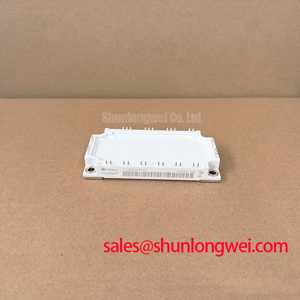
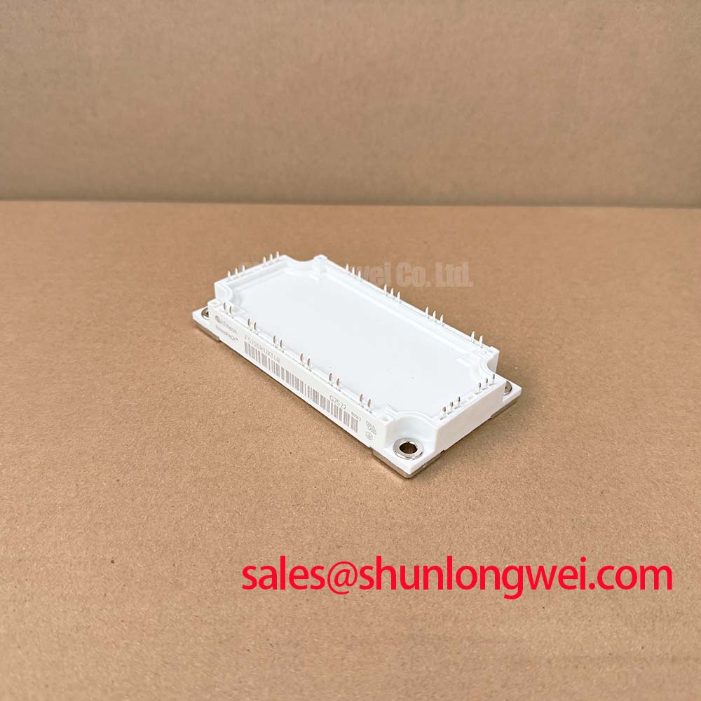
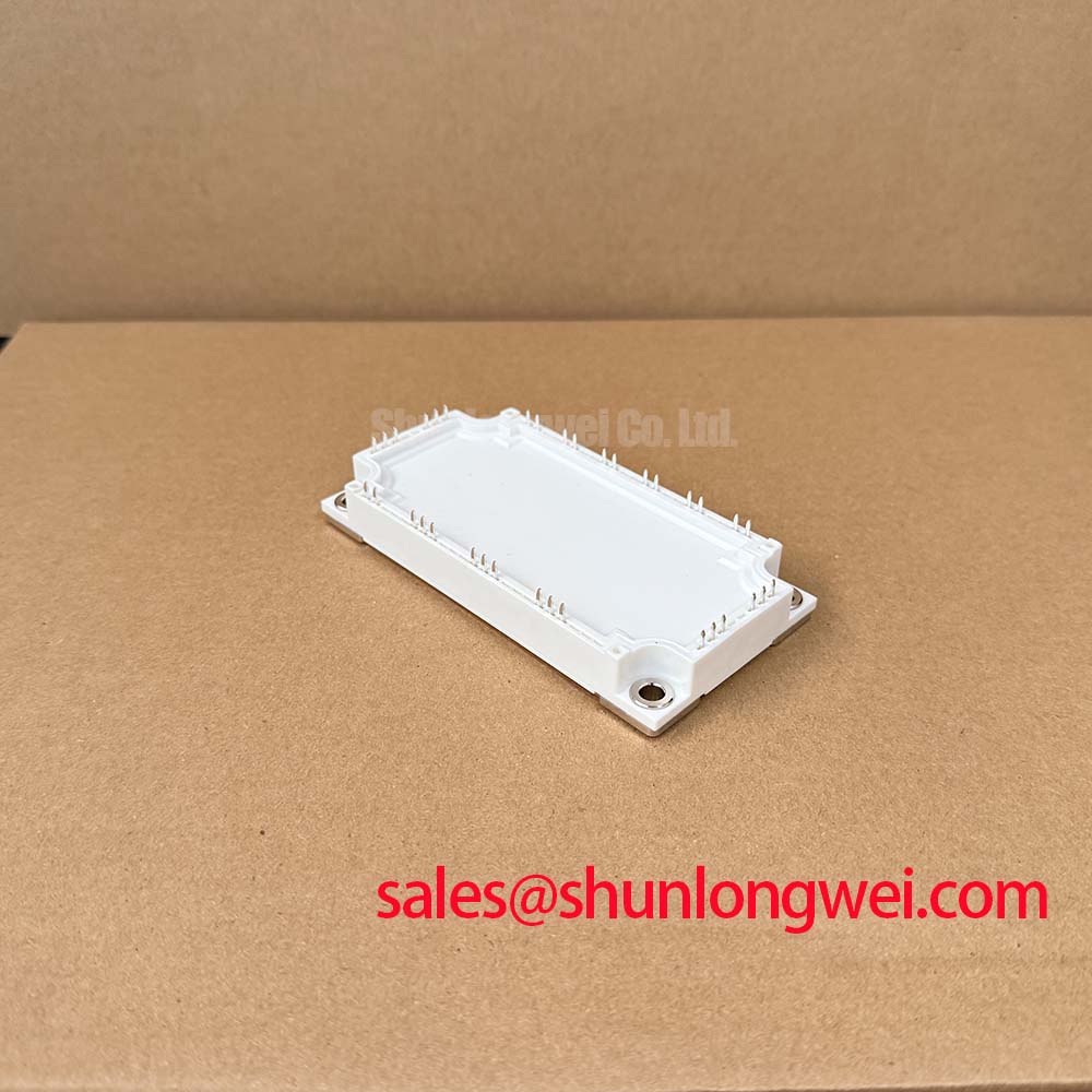
FS200R12KT4R Infineon 1200V 200A IGBT Module
The Infineon FS200R12KT4R is a 1200V, 200A sixpack IGBT module designed to optimize power conversion efficiency in high-frequency applications. Utilizing Trenchstop™ IGBT4 technology, it achieves a low typical VCE(sat) of 1.75V while maintaining a high operating junction temperature of up to 150°C. Key benefits include low conduction losses and a compact sixpack design. For engineers designing gate drivers, the integrated NTC thermistor simplifies thermal tracking. For 1200V motor drives requiring minimized switching losses at 200A, the FS200R12KT4R provides the optimal balance of efficiency and compact design.
What is the key advantage of Trenchstop™ 4 technology? It minimizes switching losses and reduces total thermal output.
How does the NTC thermistor protect the system? It monitors junction temperature to trigger overtemperature shutdown protocols.
Application Scenarios & Value
Optimizing Switching Efficiency and Thermal Management in Industrial Motor Drives
Engineers often face the challenge of heat dissipation and switching losses during rapid acceleration and deceleration cycles in motor drives. The collector-emitter saturation voltage (VCE(sat)) of 1.75 V acts like a wider water pipe, reducing electrical resistance and minimizing the power lost as waste heat during the on-state conduction phase. This efficiency is critical for maintaining thermal margins in compact cabinets where airflow is limited. In typical industrial automation applications, this sixpack configuration integrates a full three-phase inverter bridge and is widely deployed in servo drive systems, active front end (AFE) topologies, and uninterruptible power supply (UPS) units. The module enables system designs to easily comply with the IEC 61800-3 EMI standard.
For systems with lower power requirements, the related FS150R12KT4 provides a 150A alternative, while the FS100R12KT4G serves 100A designs.
Technical Deep Dive
A Closer Look at Trenchstop™ 4 Technology and Reduced Pinout Optimization
The core of this module's efficiency lies in the Trenchstop™ 4 technology, which optimizes the trade-off between switching energy and on-state voltage drop. The gate charge (Qg) of 1.65 µC can be thought of as a small capacitor cup. Gate drivers must fill this cup quickly to turn the IGBT on; a lower charge requirement allows faster gate transitions, significantly reducing the turn-on energy loss (Eon) of 20.5 mJ and turn-off energy loss (Eoff) of 18.5 mJ under high thermal stress. In terms of robustness, the design provides an outstanding Short-Circuit Withstand Time of up to 10 microseconds under worst-case fault conditions.
Furthermore, the "R" suffix designates a reduced number of pins in the EconoPACK™ 3 housing. By omitting unused terminals, the module simplifies printed circuit board routing and minimizes stray parasitic inductance to just 21 nH. This is an essential reference in our engineer's guide to IGBT modules, showing how layout optimization directly limits transient overvoltage spikes. Understanding this dynamic is crucial when decoding IGBT datasheets to select the correct gate resistors and ensure the module operates within its designated Safe Operating Area (SOA). This is a crucial parameter in power semiconductor selection when evaluating overall thermal behavior.
Key Parameter Overview
Specifications and Value Interpretation for High-Performance Power Stages
| Parameter | Specification Value | Engineering Value Interpretation |
|---|---|---|
| Collector-Emitter Voltage (VCES) | 1200 V | Provides sufficient voltage headroom for 400V AC grid applications. |
| Continuous DC Collector Current (IC) | 200 A (at TC = 95°C) | Enables reliable continuous operation under high thermal loads. |
| Collector-Emitter Saturation Voltage (VCE(sat)) | 1.75 V (typical, at Tvj = 25°C) | Minimizes static conduction losses during the on-state phase. |
| Total Power Dissipation (Ptot) | 1000 W (at TC = 25°C) | Specifies maximum safe power dissipation per switch element. |
| Module Stray Inductance (LsCE) | 21 nH (typical) | Reduces overvoltage spikes during fast turn-off switching transients. |
| Integrated NTC Thermistor (R25) | 5.00 kΩ (at TC = 25°C) | Enables real-time temperature sensing directly on the substrate. |
Download the FS200R12KT4R datasheet for detailed specifications and performance curves.
Frequently Asked Questions
Addressing Design-Phase Challenges and Operating Limits
How does the low collector-emitter saturation voltage (VCE(sat)) of 1.75 V impact heatsink selection?
Conduction losses are minimized, allowing the use of smaller, lighter heatsinks while maintaining thermal margins.
What is the practical impact of the 21 nH stray inductance on gate driver design?
Low stray inductance minimizes voltage overshoot during high di/dt switching, reducing the need for aggressive snubber networks.
What gate driver settings are recommended to manage the 1.65 µC gate charge of the FS200R12KT4R?
Using a gate voltage of +15V/-15V with a low gate resistance ensures fast transitions, keeping switching losses low.
How does the reduced pinout "R" design in the EconoPACK™ 3 housing benefit board layout?
It removes unused terminals to optimize trace routing, allowing engineers to maintain compact PCB designs with low parasitic coupling.
How does this sixpack module compare to standard modules in high-vibration environments?
Its robust copper baseplate and PressFIT-compatible mounting provide superior power cycling capability and high mechanical stability.
When integrating this module into a new design, designers should verify the gate drive loop impedance and match the NTC resistance curve (5.00 kΩ at 25°C) to the microcontroller's thermal monitoring channel. Ensuring tight gate loop routing and verifying the switching transients within the reverse bias safe operating area will secure the operational lifespan of the converter stage.