
Content last revised on September 10, 2026
Field Diagnostics & Commissioning: DC-Link Capacitance Bank Layout and Low-ES in FS200R12PT4 Topologies
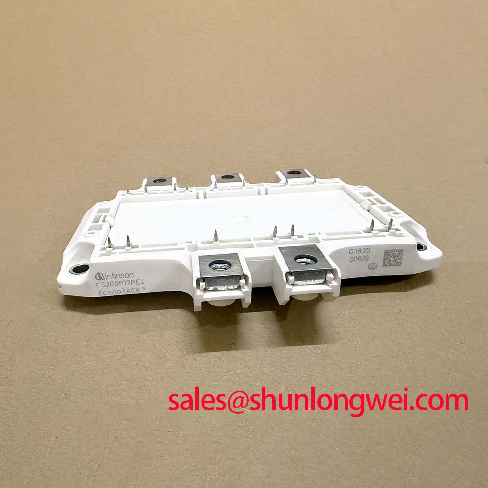
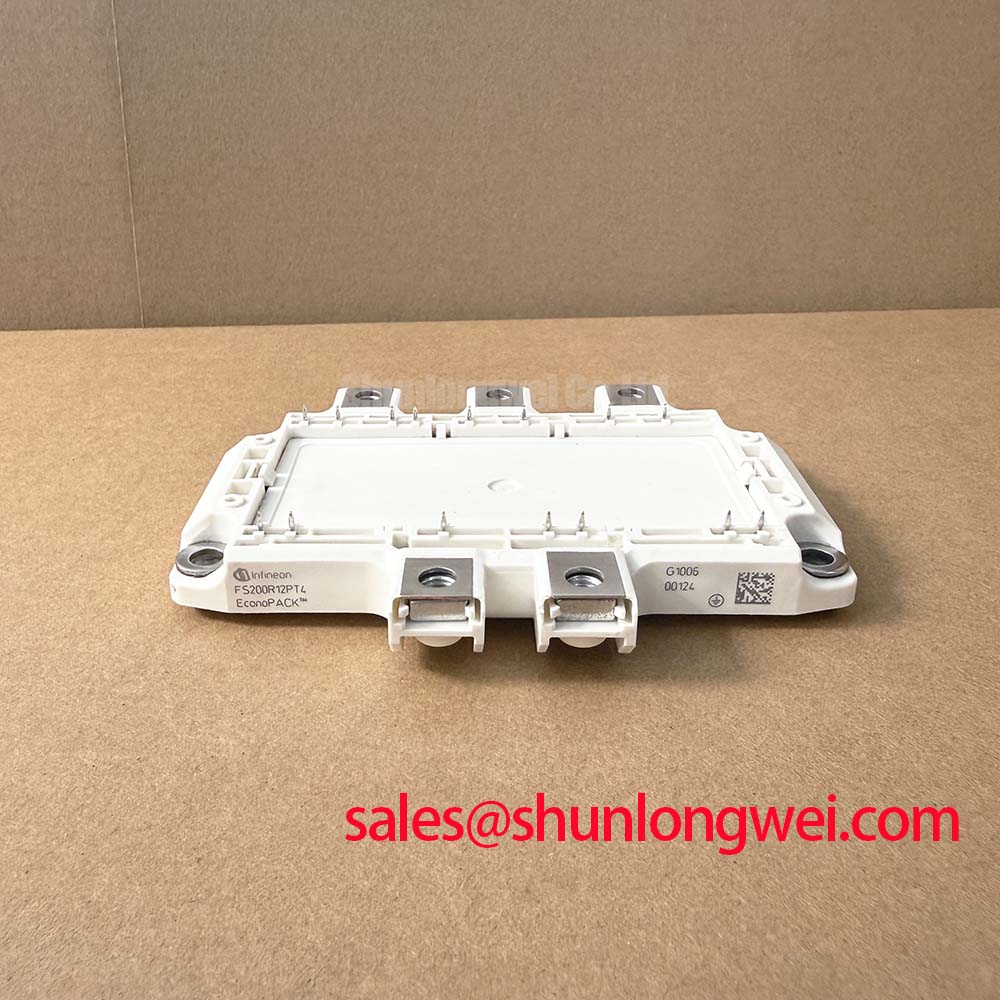
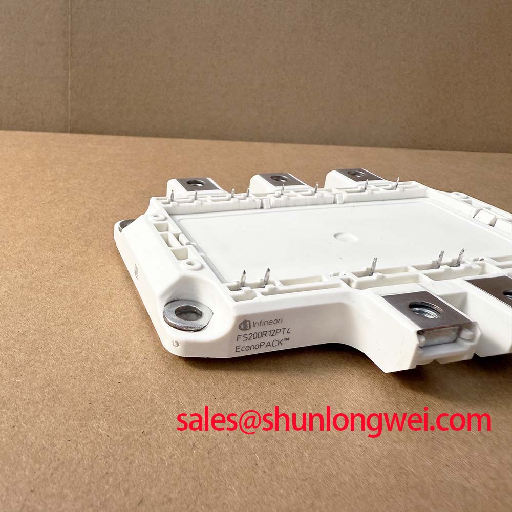
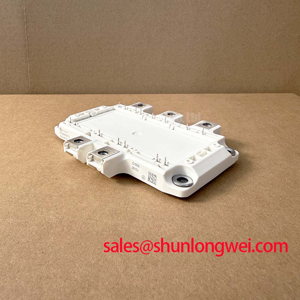
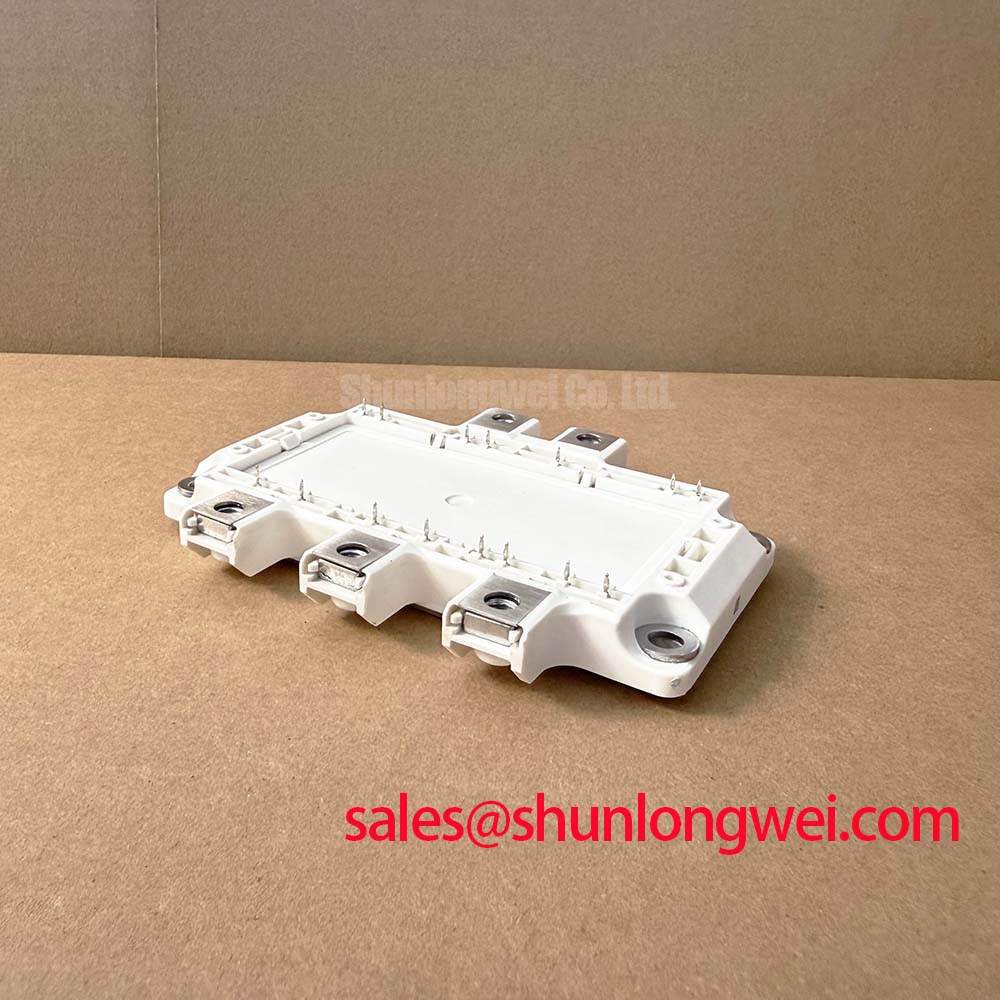
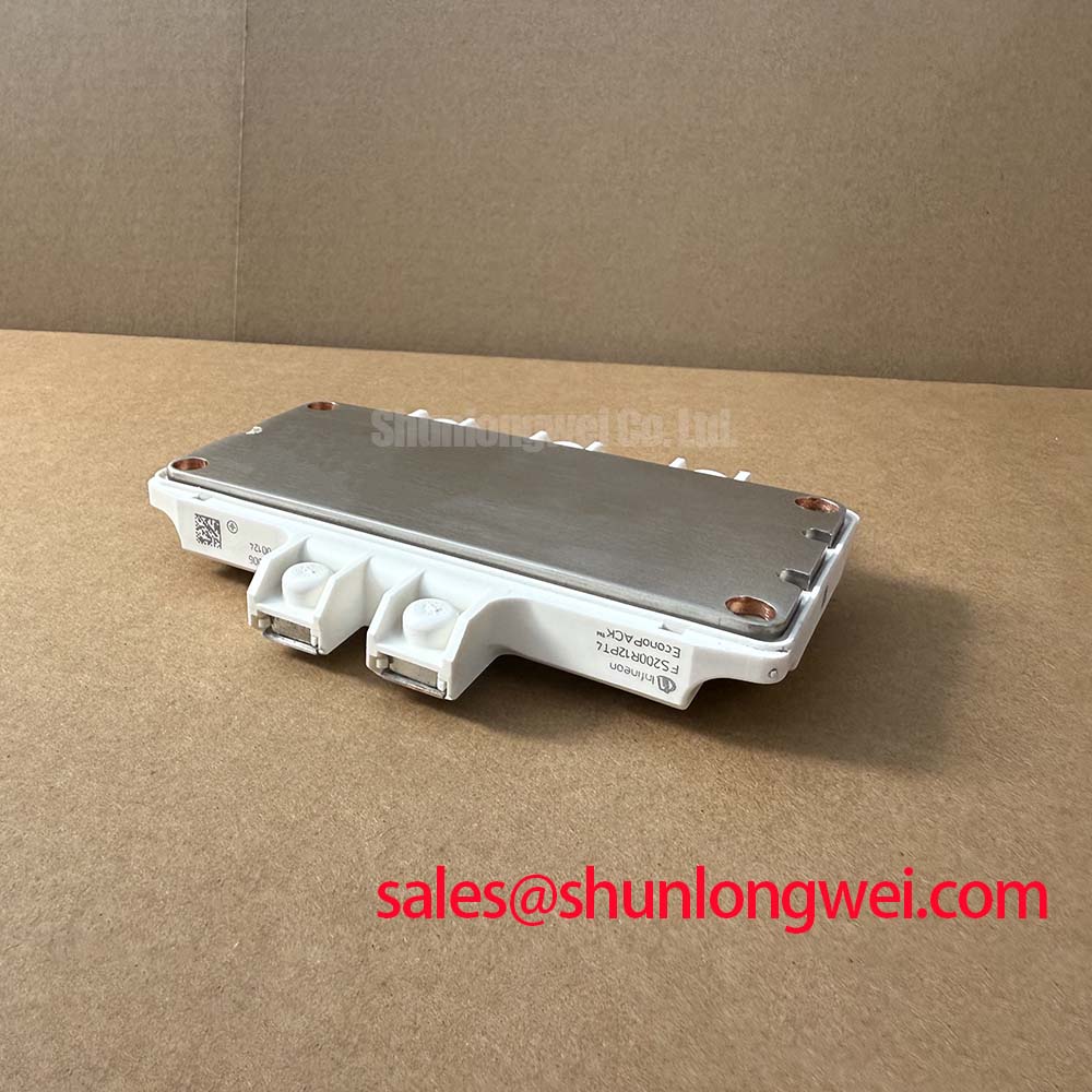
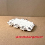
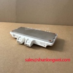
With the DC link fully discharged and locked out, first compare the power-terminal isolation condition and gate-to-emitter readings with the removed module’s documented service record before fitting an FS200R12PT4. This Infineon IGBT module is rated at 1200 V and 200 A as an Official Specification, with a Module package. Those three facts establish the initial electrical boundary, but they do not replace verification of the inverter’s bus voltage, gate-driver arrangement, cooling assembly, and protection logic.
In a bridge leg used in industrial inverter welders or medium-frequency induction heating equipment, the DC-link capacitor bank must sit electrically close to the switching loop. During turn-off, peak device voltage is influenced by the DC-link voltage plus the product of stray loop inductance and the rate of current change. This is an Engineering Calculation principle rather than a separate factory rating for the module. A long path from capacitor bank to power terminals can produce switching overshoot even when the measured DC bus is comfortably within the 1200 V module rating.
Design Consideration: keep the commutation path compact, paired, and geometrically consistent. A laminated or closely coupled bus arrangement can reduce the loop area between the DC-link capacitors and the inverter bridge. The positive and negative conductors should follow adjacent paths where practical, rather than taking separate routes around the enclosure. Snubber capacitors and MOV-based overvoltage networks should be assessed as part of the complete power stage, with their connection path kept short enough to influence the transient they are intended to control. Their required capacitance, voltage rating, pulse capability, and dissipation depend on the measured switching waveform and equipment duty cycle.
During commissioning, measure collector-emitter voltage at the module terminals with an appropriately rated differential probe and inspect the turn-off event under controlled load. A waveform that shows excessive ringing can indicate loop inductance, capacitor-bank connection resistance, an ineffective snubber path, probe placement error, or an unsuitable gate-drive setting. It should not be assigned to one cause without comparison against the known-good channel, physical layout, and switching sequence. Where the capacitor bank includes parallel capacitors, inspect each connection for uniform contact pressure and signs of heat discoloration or degraded insulation.
For service teams comparing related power-stage requirements, the FS100R12N2T4 can be reviewed as a separate 1200 V-class reference module. Its use in a particular repair remains subject to a full review of circuit topology, current demand, pin arrangement, thermal interface, and gate-driver compatibility; a shared voltage class alone does not establish interchangeability.
⚠️ Maintenance Note: Periodically monitor terminal and heatsink contact temperature during loaded operation, then clean the cooling path and recheck fastener condition during planned maintenance.
Benchtop Waveform Tuning: Mitigating Stress via Common-Mode Transient Immunity in Harsh FS200R12PT4 Installations
The FS200R12PT4 is the power switch, while immunity to common-mode transients is primarily a property of the surrounding isolated gate-driver system, its isolation barrier, PCB layout, gate-return routing, and auxiliary supply integrity. Reinforced isolation voltage and common-mode transient immunity figures must therefore be verified from the installed driver documentation. They must not be treated as factory specifications of this IGBT module.
On a bench, observe the gate-emitter waveform at the module connection points while monitoring the corresponding collector-emitter transition. A false gate pulse, a noisy off-state gate voltage, or unequal switching behavior between bridge positions can arise from common-mode coupling, a disturbed driver supply, a high-inductance gate loop, or a reference measurement problem. Compare the suspect channel with another correctly operating channel before changing components. Particular attention should be given to the gate-return conductor, which should have a deliberate low-impedance path back to the driver reference rather than sharing a disturbed high-current route.
Design Consideration: switching frequency changes the balance between conduction loss, switching loss, and heatsink capability. The permitted operating point cannot be determined from the 200 A current rating alone because it depends on semiconductor temperature, waveform conditions, modulation method, cooling-air condition, and the system’s actual load cycle. When restoring inverter welder or induction-heating equipment, engineers should capture current, voltage, and temperature behavior across the intended operating range rather than relying only on a no-load functional test.
Airflow deserves the same level of attention as the gate waveform. Dust accumulation on fins, blocked intake screens, a reversed fan, dried thermal interface material, or an enclosure that recirculates hot air can raise operating temperature without immediately causing a fault indication. Check that the heatsink seating surface is clean, flat, and free of remnants that prevent uniform contact. The thermal interface material should be applied in accordance with the original equipment’s assembly instructions; its thickness and mounting force are system-specific and should not be assumed from a generic rule.
Condensation risk also needs practical control in equipment that moves between cold storage, humid workshops, and energized production areas. Before applying power, inspect for moisture around driver boards, busbar supports, capacitor terminals, and the module mounting surface. Allowing the assembly to reach stable environmental conditions and confirming insulation integrity are sensible Engineering Recommendations, especially after extended shutdowns.
For a broader reference to power-device categories and manufacturer technology context, consult the Infineon IGBT Modules & Discretes Official Portfolio. Device portfolio information should be read alongside the exact equipment schematic and the applicable documentation for the FS200R12PT4 installation.
Transient Dynamics & Electrical Design: High dv/dt Cross-Conduction Shoot-Through on FS200R12PT4
Cross-conduction troubleshooting starts by checking whether both switches in a bridge leg receive their intended gate commands and dead-time sequence under load. An unexpected DC-link current rise or protection trip may indicate undesired turn-on, but it can also reflect a shorted load, a control timing issue, a current-sensor problem, a damaged freewheel path, or a measurement setup that does not capture the event accurately. Oscilloscope captures should include both gate-emitter voltages, DC-link voltage, and load current where safely practical.
A fast collector voltage transition can couple through device capacitances into the off-state gate circuit. If the gate circuit cannot hold the off-state device securely at its intended condition, the coupled current can lift the gate voltage and contribute to unintended conduction. Design Consideration: a dedicated active Miller-clamp function or a carefully designed low-impedance gate discharge path can help control this mechanism, provided that the driver and module terminal configuration support the approach. The actual gate bias, gate resistance, clamp behavior, and dead-time setting must be selected and verified by the system designer from measured waveforms and the relevant device documentation.
Do not judge gate-drive health from controller output alone. A gate pulse can look clean at the driver connector while its shape is degraded at the module because of connector resistance, damaged cable shielding, excessive loop area, poor solder joints, or a shared emitter return. Test probes themselves can alter or misrepresent a high-speed measurement when their reference lead arrangement is unsuitable. Repeat measurements with a validated probing method and compare against a known-good power leg before interpreting ringing as a device failure.
When a power stage uses several modules in parallel, the positive temperature coefficient behavior associated with IGBT conduction can assist static current sharing under suitable conditions, but it does not guarantee dynamic sharing. Physical conductor symmetry, matched driver paths, equal thermal coupling, and simultaneous switching behavior remain important. Design Consideration: each parallel path should be assessed for current distribution during the actual transient, not only at steady load. The module’s rated current is not a blanket approval for any parallel topology or duty profile.
In inverter welder and induction-heating repairs, confirm that the load network has not changed from the original electrical condition. Loose output connections, altered resonant components, or a failed auxiliary rectifier can change current phase and switching stress. The FS200R06KL4 may be relevant for review where an associated rectifier or auxiliary power-stage position is present, but its suitability must be determined from the original circuit function and ratings rather than assumed from its presence in a related equipment family.
FS200R12PT4 Circuit Protection & Reliability: Calibrating Braking Resistor Sizing and Chopper Transients
In a regenerative DC-link arrangement, the braking chopper and braking resistor are system-level elements that limit bus-voltage rise by converting returned mechanical energy into heat. The FS200R12PT4 has an Official Specification of 1200 V and 200 A, yet those ratings do not define the required braking-resistor value, pulse-energy capability, chopper-switch current, or control threshold. These values must be derived from the DC-link capacitance, deceleration profile, motor or load energy, resistor thermal capacity, enclosure ventilation, and measured switching behavior.
A failed chopper circuit can present itself as DC-link overvoltage during deceleration, but diagnosis should remain evidence-led. Inspect the brake resistor connection, resistor housing, wiring insulation, chopper gate command, current path, and voltage-sensing circuit. Verify whether the control system is actually requesting braking and whether the chopper responds correctly under a controlled test. A resistor that has changed value, a poor terminal joint, a broken sense connection, or an incorrectly timed command can each alter the observed bus response.
MOV coordination also requires an equipment-level review. An MOV can absorb brief surge energy when selected for the application, but it is not a substitute for a properly designed commutation loop, capacitor bank, snubber arrangement, or braking path. Its clamping characteristic, energy capability, installation position, and end-of-life condition should be checked against the original design. Any replacement must be evaluated for the actual transient energy and safety requirements of the equipment.
At planned shutdown intervals, inspect the module terminals, capacitor busbars, braking-path connections, fan wiring, and driver-board connectors for discoloration, looseness, contamination, or moisture exposure. Repeated thermal cycling can affect contact interfaces over time, so a torque audit should follow the equipment manufacturer’s mechanical instructions rather than an assumed universal value. After service work, perform a controlled recommissioning sequence that verifies gate timing, DC-link behavior, cooling operation, and protection response before returning the system to production duty.
For system-level discussion of selection factors and reliability practices, the Power Electronics Masterclass provides related engineering context. It should support, rather than replace, the measurements and original design documentation required for the specific FS200R12PT4 power stage.