
Content last revised on September 12, 2026
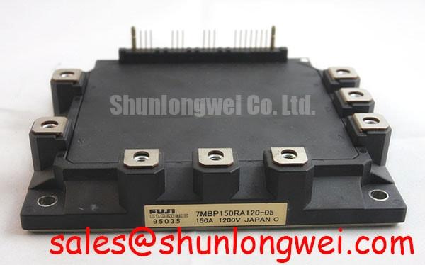
Before energizing a replacement assembly, verify the nameplate rating, inspect the package and terminals, and compare cold resistance readings with a known good unit using an isolated meter test. The FT150R12KE3G_B4 is an Infineon IGBT module specified for high power switching applications where voltage margin, thermal transfer, and controlled gate drive behavior must be checked at system level.
| Technical Metric | Value | Engineering Value |
|---|---|---|
| Collector Emitter Voltage, VCES | 1200 V | Provides voltage overhead for 400 VAC line based systems, subject to DC link transient verification |
| Continuous Collector Current, IC | 150 A | Supports high power delivery in heavy duty automated equipment |
| Collector Emitter Saturation Voltage | 1.7 V | Helps control static conduction loss under the specified test conditions |
| Thermal Resistance, RthJC | 0.18 K/W | Supports heat transfer from the junction to the case through the approved thermal interface and heatsink assembly |
| Maximum Power Dissipation, Ptot | 700 W | Defines the stated power dissipation boundary for thermal design evaluation |
These values are official specification data supplied for this product page. They do not replace the complete Infineon datasheet, switching waveform limits, safe operating area information, gate drive requirements, or the thermal interface instructions applicable to the exact production revision. Engineers evaluating this module for electric material handling equipment should verify the original inverter topology, DC bus voltage, switching frequency, braking duty, cooling method, and protection circuit before commissioning.
FT150R12KE3G_B4 Operational Boundaries: Evaluating Dynamic Braking Chopper Operation Limits
In a forklift traction inverter, the braking chopper transfers regenerative energy from the motor into a ballast resistor when the DC link rises during deceleration. The module selection cannot be based on collector current alone. The engineering review should compare the resistor pulse energy, braking duration, repetition pattern, DC link operating range, and available cooling against the module’s 1200 V VCES, 150 A IC, and 700 W Ptot ratings.
A practical commissioning sequence begins with the power stage disabled. Inspect the braking resistor, chopper loop, snubber components, busbar joints, and gate driver supply. After low voltage gate verification, use an isolated differential probe to observe collector emitter voltage during controlled switching. The measured peak must be assessed against the DC link and transient design margin; the module rating alone does not establish immunity to every wiring induced overshoot.
Minimize the commutation loop formed by the module, braking resistor, capacitor bank, and return busbar. A laminated or closely coupled bus structure can reduce parasitic inductance, while symmetrical current paths help prevent localized heating. Clearance and creepage must be checked against the actual working voltage, pollution environment, insulation system, and applicable equipment standard rather than copied from a generic layout.
The resistor network also requires independent review. Its thermal mass may tolerate a short regenerative pulse while still overheating under repeated warehouse duty cycles. Log DC link voltage, braking current, resistor temperature, and fault timing during a representative loaded test. A chopper fault may involve the gate driver, resistor, DC link capacitor, current feedback, or mechanical load, so each signal should be checked against the known good inverter waveform.
FT150R12KE3G_B4 Thermal Electrical Optimization: High Speed Fault Management and VCE Desaturation Tuning
Desaturation protection is commonly used to detect a rapid rise in collector emitter voltage while the gate command remains active. The required detection delay, blanking interval, fault threshold, and soft turn off profile are system and driver design parameters. The supplied product data does not establish a universal sub 10 microsecond protection setting or a guaranteed short circuit withstand interval for every operating condition, so these values must be taken from the applicable Infineon documentation and validated with controlled testing.
A two stage turn off strategy is a Design Consideration for limiting current interruption stress. The first stage reduces gate drive strength or current slew, and the second stage completes turn off after the driver confirms a fault condition. The selected sequence must be coordinated with the module’s gate charge, stray inductance, driver propagation delay, and DC link voltage. Oscilloscope measurements should capture gate emitter voltage, collector emitter voltage, collector current, and the fault signal on the same time base.
Parallel module operation demands matched electrical paths. At operating currents where the IGBT’s temperature behavior supports static current sharing, this characteristic does not remove the need for equal busbar geometry, closely matched gate impedance, and coordinated thermal coupling. Compare current sharing during startup, steady traction load, and regenerative braking. Unequal switching waveforms may indicate gate loop coupling, emitter path imbalance, driver timing mismatch, or probe reference error.
For broader platform context, engineers can review the Infineon EconoDUAL 3 product information and the manufacturer’s High Power Semiconductor Solutions. These references provide family level application context and should not be interpreted as a substitute for the exact electrical and mechanical data of this part number.
Field Diagnostics and Commissioning: DC Bus Operating Voltage Headroom Derating in FT150R12KE3G_B4 Topologies
When this module is evaluated above normal installation altitude, the design review should consider both reduced air insulation capability and environmental changes in cooling. Terrestrial neutron exposure and Single Event Burnout risk are reliability topics requiring device specific qualification data, mission profile information, and an appropriate reliability methodology. No universal FIT rate or altitude derating value should be assigned to this module without an authoritative source.
The field engineer can still perform useful checks. Record the measured DC bus range during charging, traction acceleration, plugging, and regenerative braking. Capture switching overshoot at the module terminals, inspect the snubber and MOV network for thermal damage, and verify that the protective clamp voltage remains compatible with the IGBT voltage boundary. MOV selection is a system coordination task involving surge energy, repetition, clamping behavior, and capacitor impedance.
Reverse recovery in the freewheel diode can influence current commutation, voltage overshoot, and radiated noise. The diode’s recovery softness and the complete commutation loop should be verified from the applicable datasheet and switching test results. If EMI changes after a module replacement, compare gate timing, busbar position, diode current, resistor values, and chassis bonding before assigning the issue to the IGBT itself.
Mechanical thermal performance also affects electrical reliability. The heatsink surface, interface material, clamping arrangement, and pressure distribution should follow the manufacturer’s mechanical instructions. For flat pressure mounted assemblies, a calibrated fastening method and, where specified by the equipment design, disc spring loading can help maintain even contact across both cooling surfaces. The actual fastener method and torque remain installation specific.
For a neutral comparison point during sourcing, engineers may review FZ800R12KS4_B2, then confirm voltage class, current capability, package geometry, pin arrangement, thermal data, and gate drive compatibility before considering any alternative.
FT150R12KE3G_B4 Operational Boundaries: Evaluating Differential Gate Emitter Loop Routing
The gate driver should reference the module’s intended auxiliary emitter return rather than sharing a long, high current emitter path. Separating the auxiliary control return from the main power emitter trace reduces mutual coupling and makes the sensed gate emitter voltage more representative of the driver output. This is a Design Consideration, not a substitute for the exact terminal definition and application circuit in the manufacturer’s documentation.
Route the gate command and auxiliary emitter return as a compact differential loop, away from the collector busbar and high di/dt commutation path. Avoid routing the driver return through contactors, shunts, laminated busbar joints, or other conductors carrying switching current. The gate resistor, protection components, and driver reference should be placed so that the loop is short and mechanically stable. Designers should verify ringing and Miller induced movement directly at the module terminals.
During troubleshooting, compare the gate emitter waveform at the driver board with the waveform measured at the module. A difference between these locations may indicate common emitter inductance, connector impedance, probe ground error, or an unstable driver supply. Check turn on and turn off transitions at several load currents, then confirm that the gate remains firmly controlled while the opposite switch changes state.
💡 Pro Tip: Disconnect the DC link and allow the equipment discharge process to complete before inserting or removing gate driver and power connections.
When the application includes a thyristor controlled charging or precharge path, the SCR gate trigger circuit must be evaluated separately using the device’s specified IGT, VGT, pulse duration, and repetition requirements; those characteristics are not established by the IGBT module data above. For additional power semiconductor design context, see Wide Bandgap Revolution.