

Content last revised on October 18, 2026
Preventing Spurious Faults: Dynamic Firing Delay Angle Adjustment Guidelines for MCMA260PD1600YB
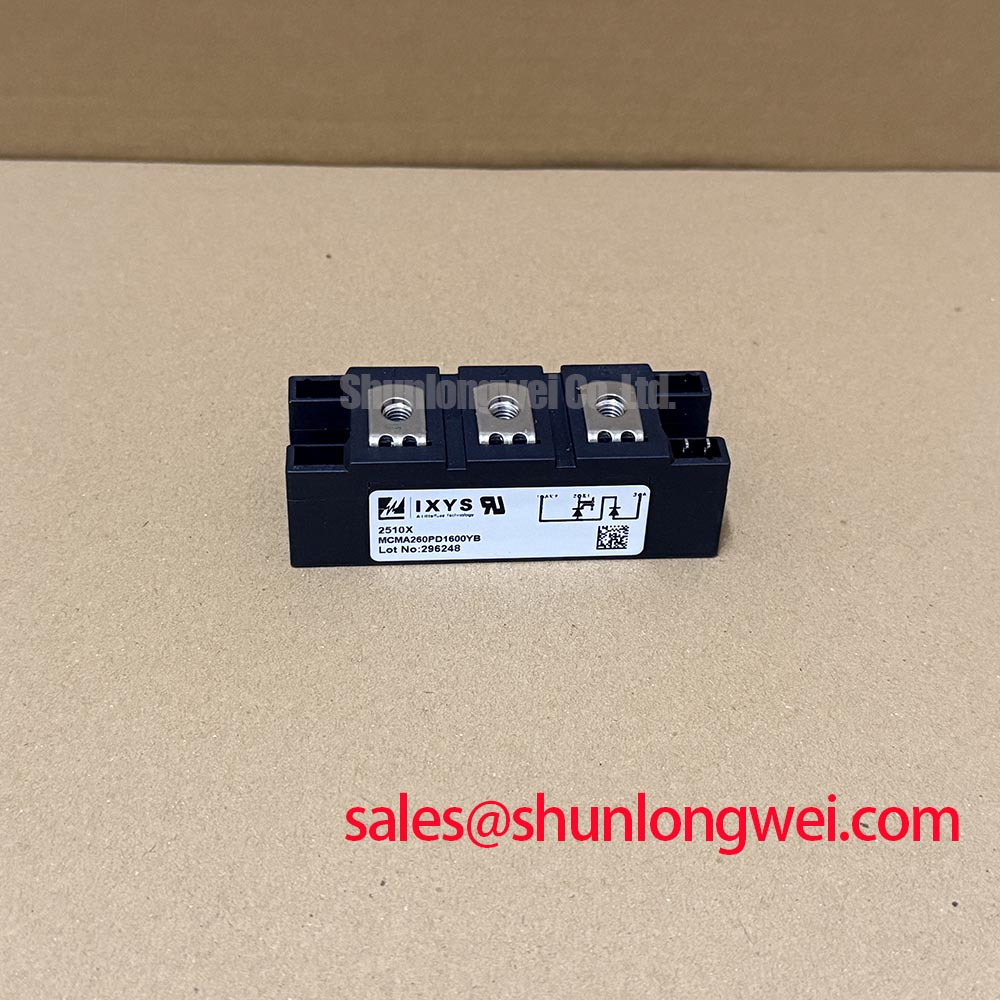
| Manufacturer | IXYS |
|---|---|
| Part Number | MCMA260PD1600YB |
| Product Category | Dual Thyristor Module |
| Rated Voltage | 1600.0 V |
| Rated Current | 412.0 A |
| Package | TO-240AA |
Measure the gate and main terminal paths with the module isolated, then compare the cold-state readings with a known-good unit before investigating firing-angle faults in a grid-tied static Var compensator or thyristor-switched capacitor bank.
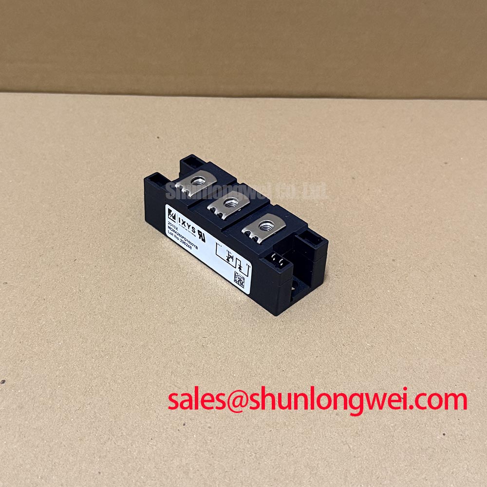
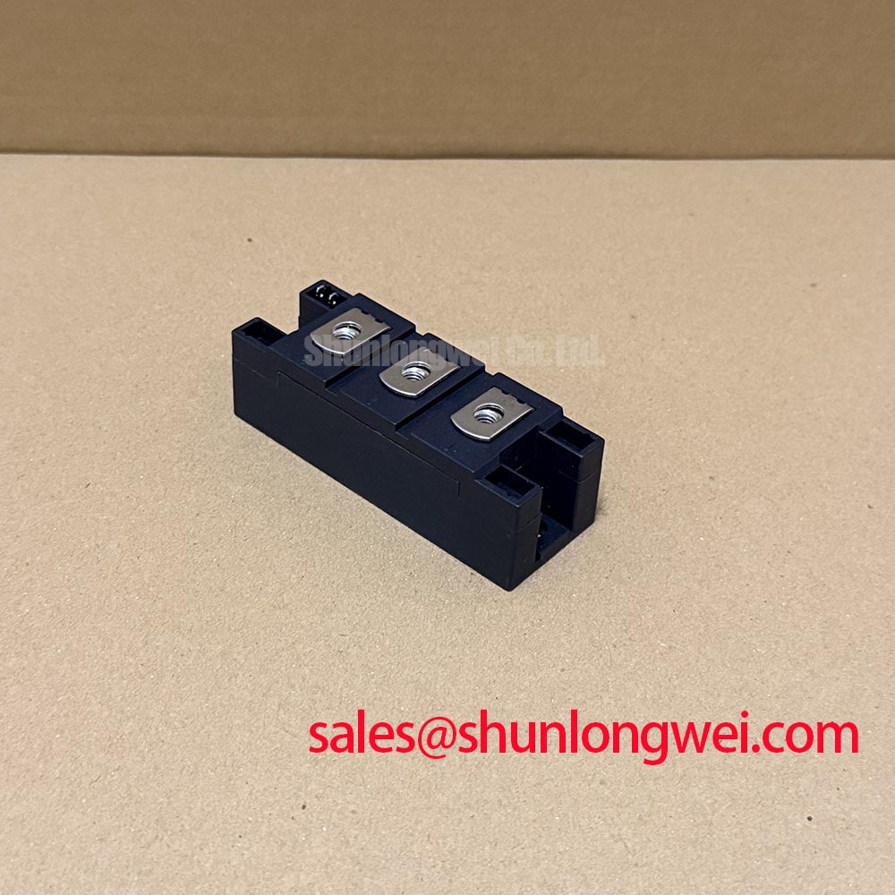
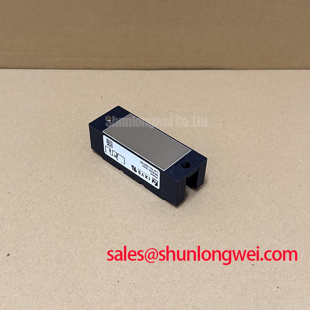
The MCMA260PD1600YB is an IXYS dual thyristor module rated at 1600.0 V and 412.0 A, housed in a TO-240AA package. These are official product specifications; they do not define the complete operating limit of an assembled SVC branch. The firing controller, line impedance, commutation conditions, protection fuse, cooling system, and switching sequence must be evaluated together.
When a firing-angle adjustment produces unexpected current pulses, check the controller timing at the gate terminals and compare it with the corresponding anode and cathode waveform. A delayed or inconsistent gate signal may result from the driver supply, isolation stage, wiring inductance, or control reference rather than the thyristor module itself. Designers should verify the required gate trigger conditions from the original IXYS documentation for this exact device revision.
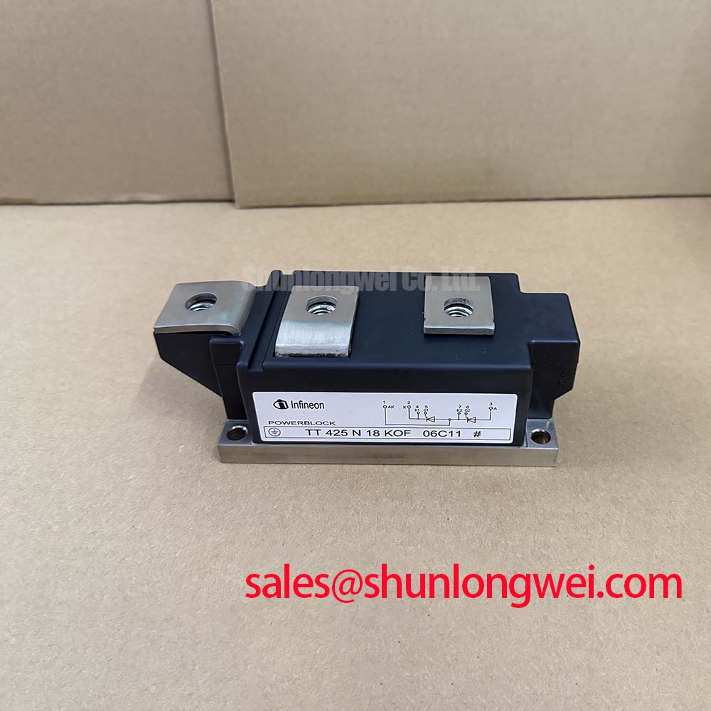
For a neutral comparison during procurement, engineers may also review the TT500N18KOF. It should be treated as a separate device for electrical, mechanical, thermal, and gate-drive validation rather than as an automatic replacement.
MCMA260PD1600YB Operational Boundaries: Evaluating Turn-On Current Rise Limiting
Capture the current and voltage waveforms at the module terminals when a suspected false turn-on occurs, checking whether the event coincides with commutation overlap, a control transition, or a rapid change on the main power circuit.
RC snubbers and series saturable reactors are system-level protection elements. Their values cannot be assigned from the voltage and current ratings alone. A suitable network depends on the actual circuit inductance, capacitor bank configuration, line frequency, switching sequence, thyristor recovery behavior, and measured transient waveform. As a Design Consideration, the snubber should reduce unwanted voltage transients without creating excessive reactive current or repetitive power loss.
The same principle applies to turn-on current rise limiting. A reactor or other current-limiting element should be selected from the complete branch impedance and the permitted semiconductor stress. The resulting performance must be confirmed during controlled switching tests by checking peak current, current rise behavior, voltage overshoot, and thermal response.
Do not infer a gate threshold, gate pulse current, critical rate of voltage rise, or critical rate of current rise from the 1600.0 V and 412.0 A ratings. Those values require the manufacturer’s electrical characteristic tables. A front-end supply or rectifier stage may be evaluated alongside devices such as SSIL2890S46C, but each component must retain its own verified ratings and application conditions.
Assembly Integrity and Layout Architecture: Implementing Semiconductor Protection Fuse Selection for MCMA260PD1600YB
Inspect every power connection for correct polarity, clean contact surfaces, secure clamping, and adequate clearance before energizing a repaired SVC or capacitor-switching assembly.
Semiconductor fuse coordination requires the fuse clearing I²t to be compared with the applicable thyristor surge and short-circuit withstand data from the manufacturer’s documentation. The available voltage, current, and package information confirms the identity of this module but does not provide a valid fuse I²t coordination value. Selecting a fuse from the continuous current rating alone can leave the silicon exposed during a dead-short event.
During layout review, keep the high-current path short and symmetrical where practical, separate gate wiring from high dv/dt conductors, and verify that the enclosure maintains the required creepage and clearance for the working voltage and pollution environment. These are Design Considerations, not official mechanical specifications for this module. The system engineer must confirm the final insulation distances against the applicable equipment standard.
The thyristor semiconductor standard IEC 60747-6 provides relevant terminology and test framework for thyristor devices. It does not replace the device-specific IXYS data required for fuse selection, surge-current coordination, or insulation validation.
💡 Bench Tip: Use ESD protection and record the cold-state terminal readings before connecting the module to the powered control or gate circuit.
MCMA260PD1600YB Thermal-Electrical Optimization: Gate Trigger Current and Temperature Practical Tuning
Probe the gate drive directly at the module terminals and compare the pulse shape at cold start and operating temperature when a thyristor appears to trigger inconsistently.
Gate pulse timing, pulse duration, trigger-current margin, holding behavior, and temperature response must be tuned from the original IXYS electrical characteristics and the actual driver circuit. A multi-pulse strategy may be considered when the control topology requires greater firing reliability, but it should be validated against driver isolation capability, common-mode transients, gate wiring layout, and thermal conditions.
For an industrial drive or SVC control board, optical isolation and digital isolators should be checked for common-mode transient behavior under the real switching waveform. A control signal that appears correct at the controller may be distorted at the module because of isolation capacitance, grounding impedance, or gate-loop coupling. Oscilloscope verification at the module terminals is the practical way to separate a driver problem from a power-device problem.
Thermal evaluation should include the module mounting surface, heatsink interface, airflow or coolant path, and the actual conduction pattern of both internal thyristor paths. Do not assign a junction temperature, mounting torque, thermal resistance, or gate current value without the applicable IXYS datasheet revision. The broader principles of wide-bandgap switching and transient control can be reviewed in Wide Bandgap Revolution, while the present device remains a silicon thyristor module requiring its own verified data.