

Content last revised on September 25, 2026
Preventing Spurious Faults: DC Bus Operating Voltage Headroom Derating Guidelines for MG800J1US51
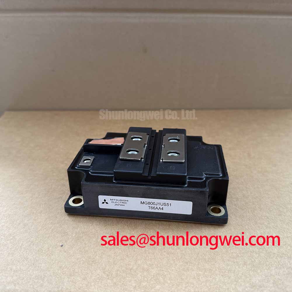
Before fitting the MG800J1US51, isolate the converter, discharge the DC link under the site procedure, inspect the power terminals and gate connections for mechanical damage, then compare the installed unit’s rating label against the required 600V collector-emitter voltage rating and 800A collector-current rating under the specified conditions.
The Toshiba MG800J1US51 IGBT module is specified with VCES = 600V, IC = 800A, and VGES = ±20V as Official Datasheet Specifications. Its stated typical collector-emitter saturation voltage is 2.1V. Typical switching data lists a 0.8µs turn-on time and 1.5µs turn-off time. The specified isolation withstand voltage is 2500V AC for 1 minute.
| Official Specification | Value |
|---|---|
| Collector-Emitter Voltage, VCES | 600V |
| Collector Current, IC | 800A |
| Gate-Emitter Voltage, VGES | ±20V |
| Collector-Emitter Saturation Voltage, VCE(sat) | 2.1V typical |
| Collector Cut-Off Current, ICES | 2.0mA maximum |
| Turn-On Time, ton | 0.8µs typical |
| Turn-Off Time, toff | 1.5µs typical |
| Isolation Voltage, Visol | 2500V AC for 1 minute |
Start every converter repair by checking the actual DC bus waveform at the module location, rather than relying only on the controller display or the nominal rectifier voltage. The 600V VCES rating is an Official Datasheet Specification for the MG800J1US51. It does not by itself define the acceptable DC bus setting, switching overshoot, cable reflected voltage, or surge margin of a complete converter. Those limits depend on the busbar geometry, capacitor location, snubber condition, operating current, switching behavior, and controller protection response.
For full-scale wind turbine converters, technicians should capture the DC bus during normal load transitions, grid events, and controlled shutdown events where permitted by the site procedure. A transient peak near the module can differ materially from the voltage measured at a remote DC link capacitor bank. Check whether MOV devices, RC snubbers, and capacitor connections are still physically sound and electrically connected. A damaged MOV, degraded snubber capacitor, loose laminated busbar fastener, or high-resistance capacitor joint can all contribute to voltage spikes, but each condition requires measurement before assigning a cause.
High-altitude operation deserves separate system review. Terrestrial neutron exposure, altitude-related insulation coordination, and semiconductor single-event behavior are high-risk reliability subjects. No single-event burnout rate, FIT rate, altitude capability, or required DC bus derating value is stated here for the MG800J1US51. Design Consideration: where a converter operates above typical terrestrial conditions, the system engineer should evaluate the applicable equipment standard, location profile, converter voltage stress, protection response, and manufacturer-level reliability evidence before approving an operating limit.
Clearances around energized buswork should remain free from conductive debris, moisture paths, and displaced insulation. During a service intervention, inspect for tracking marks around terminals and confirm that protective covers have returned to their intended positions. This is especially relevant when a converter cabinet has experienced vibration, condensation, or repeated thermal cycling.
⚠️ Field Alert: Tighten power connections only to the equipment manufacturer’s specified torque and apply thermal interface material as an even, thin layer before clamping the module to its cooling surface where specified by the module and cooling-assembly manufacturer.
Where a lower-current device is being reviewed as a reference during an assembly audit, the MG100Q1ZS40 should be treated as a separate model requiring independent checks of voltage rating, current capability, package interface, gate-drive requirements, and converter qualification.
MG800J1US51 Circuit Protection & Reliability: Calibrating Common-Mode Transient Immunity in Harsh Industrial Drives
The MG800J1US51 has an Official Datasheet Specification of 2500V AC isolation for 1 minute. This value must not be represented as a reinforced isolation classification, a system safety certification, or proof of a particular common-mode transient immunity level. No claim of insulation performance above the stated value, including a specific CMTI threshold, should be inferred from the module rating alone.
When nuisance trips or unexpected gate activity appear after a module replacement, examine the full gate-drive path. Check the driver supply stability, isolated driver wiring, gate-return routing, optocoupler or digital-isolator behavior, fault-output reference, and the location of any gate-emitter sensing connection. A gate pulse that looks correct at the driver board can become distorted at the module terminals when the return path shares high-current switching inductance.
Engineering Recommendation: keep the gate-drive loop compact and route its return with the associated gate signal so that power-loop current does not impose unwanted voltage on the driver reference. The objective is to reduce false turn-on risk during rapid collector-voltage transitions. Oscilloscope verification at the actual module gate and emitter points, using safe differential measurement methods, should determine whether observed pulses are a driver issue, a layout issue, or a measurement artifact.
Phase-angle control, line-frequency ripple, and DC-link energy storage are converter-level functions. Their effect on current stress should be verified from the actual converter topology and control behavior. RC snubbers and MOV networks can limit selected transient conditions, but component values, energy ratings, and placement must be determined by the system design and confirmed through switching tests. The module’s typical 0.8µs turn-on and 1.5µs turn-off characteristics provide useful timing context, not a universal dead-time prescription.
For broader context on heat paths, mounting interfaces, and cooling architecture, see The Advanced Thermal Management Revolution. Cooling construction and thermal resistance must still be verified for the actual converter assembly rather than assumed from a general technical discussion.
Preventing Spurious Faults: Static and Dynamic Current Distribution Guidelines for MG800J1US51
When multiple power paths operate in parallel, begin with physical symmetry before changing control settings. Compare conductor lengths, busbar overlap, terminal contact condition, gate-resistor placement, gate-return routing, cooling contact, and airflow or coolant distribution. Static current sharing and dynamic switching current sharing are related but different problems. A balanced DC-resistance path does not guarantee balanced switching behavior.
The 2.1V typical VCE(sat) value is an Official Datasheet Specification for the MG800J1US51 under the manufacturer’s stated test conditions. It is not a field acceptance threshold and should not be used as a direct multimeter pass-or-fail value. Under operating load, the collector-emitter voltage changes with current, junction temperature, gate-drive conditions, and switching state. Compare equivalent positions under equivalent measured conditions, preferably against known stable phases within the same converter.
IGBT temperature behavior can influence steady-state sharing in parallel arrangements, while unequal gate-loop inductance and drive propagation can shift current dynamically during turn-on and turn-off. Design Consideration: match gate-loop geometry as closely as the mechanical layout allows, minimize parasitic inductance, and verify current balance with appropriate isolated current measurement during representative switching tests. The final balance assessment remains system determined because control timing, load inductance, switching frequency, and thermal conditions all influence the result.
If one phase reports excessive current or repeated desaturation protection, inspect the current-sensor chain and gate-drive supply before declaring the module defective. Confirm the correct phase connection, check that the command and feedback references are intact, and compare waveforms with a known healthy channel. An abnormal reading may indicate a sensing issue, a connection issue, a gate-drive mismatch, or actual power-stage stress.
The general relationship between conduction loss and collector current means that even small distribution differences can become thermally significant in a high-current converter. The intended practical response is measurement-based correction of mechanical and electrical symmetry, not a universal gate-resistor or timing value.
MG800J1US51 Thermal Electrical Optimization: Suppressing Cres-Induced Gate Voltage Spikes Through Practical Tuning
After confirming correct terminal connections, inspect the gate waveform during the opposite-switch transition. A collector-voltage swing can couple through the device capacitances and raise the gate voltage of the inactive IGBT. If this creates unintended conduction, the converter can show overcurrent alarms, distorted phase current, or protection trips. These symptoms require waveform evidence because similar alarms can also originate in the load, sensor circuit, controller logic, or DC link.
The MG800J1US51 gate-voltage limit is ±20V as an Official Datasheet Specification. The gate driver must keep the terminal voltage within that limit under all expected operating and fault conditions. A dedicated Miller clamp or negative gate bias can be considered as a system-level mitigation where measured switching transients show a false turn-on risk. The appropriate method, bias level, driver capability, and clamp behavior are determined by the gate-driver design and must be validated at the module terminals during switching tests.
Pay close attention to the physical separation between the high-current commutation path and the low-energy gate path. The goal is to avoid injecting power-loop voltage into the gate reference while suppressing turn-off overshoot. Check whether the gate return is connected through a shared power conductor, whether the driver-board connector has loosened, and whether an added repair wire has created a large loop. Correcting a poor return path often produces a more useful result than changing multiple gate-drive components without measurement.
Thermal and electrical checks should proceed together. The typical saturation voltage, switching timing, cooling-interface condition, and phase-current waveform form a practical set of observations for assessing the installed module. Toshiba device behavior can be compared with general IGBT switching principles discussed by Mitsubishi Electric CSTBT™ Technology, while recognising that device technologies, ratings, and application conditions are not interchangeable.
For a wind turbine full-scale converter or another industrial power stage, verify the original gate-drive polarity, interlock logic, protection thresholds, and cooling-assembly documentation before returning the equipment to service. The MG800J1US51 should be assessed as a 600V, 800A Toshiba IGBT module within the electrical, thermal, and protection boundaries of the existing system.