Content last revised on September 10, 2026
Assembly Integrity & Layout Architecture: Implementing DC Link Capacitance Bank Layout for 2MBI200SB-120-50
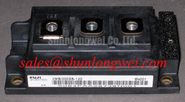
With the DC link fully discharged, begin incoming inspection by checking the terminal arrangement against the original inverter schematic, then compare cold-state diode-test readings between equivalent power paths before mounting the 2MBI200SB-120-50. A diode-test reading is useful as a comparative check when applied consistently across matching terminals, but it must be interpreted with the module circuit diagram and the known condition of the surrounding assembly. A reading that differs from the corresponding path may justify further checks of the module, gate-drive board, busbar hardware, and connected snubber network.
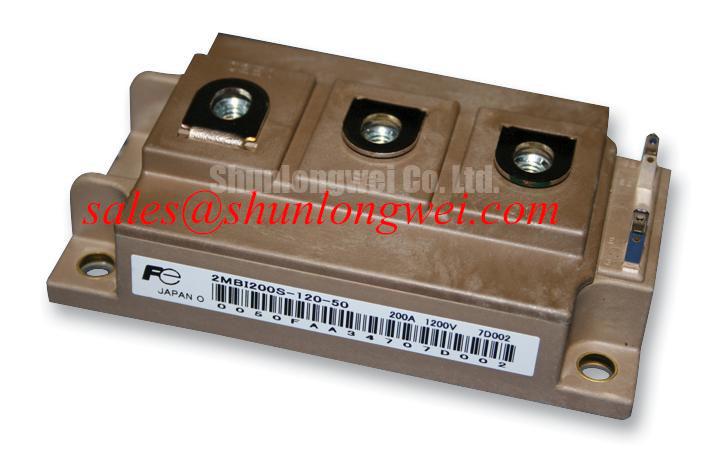
This Fuji Electric IGBT module is officially rated at VCES 1200 V at Tj = 25°C and IC 200 A at TC = 80°C. Its published collector-emitter saturation voltage is 2.6 V typical and 3.2 V maximum, specified at IC = 200 A, VGE = 15 V, and Tj = 125°C. These conditions matter during repair assessment because a bench measurement made at low current and room temperature cannot be treated as a substitute for the published high-current switching specification.
| Official Datasheet Specification | Value | Specified Condition |
|---|---|---|
| Collector-emitter voltage, VCES | 1200 V | Tj = 25°C |
| Continuous collector current, IC | 200 A | TC = 80°C |
| Collector-emitter saturation voltage, VCE(sat) | 2.6 V typical / 3.2 V maximum | IC = 200 A, VGE = 15 V, Tj = 125°C |
| Turn-on switching loss, Eon | 38 mJ per pulse | VCC = 600 V, IC = 200 A, Tj = 125°C |
| Turn-off switching loss, Eoff | 45 mJ per pulse | VCC = 600 V, IC = 200 A, Tj = 125°C |
| Junction-to-case thermal resistance | 0.083 °C/W per IGBT | Official datasheet specification |
| Short-circuit withstand time, tsc | ≥10 µs | VGE ≤ 15 V, VCC ≤ 800 V, Tj ≤ 125°C |
| Maximum junction temperature, Tjmax | 150°C | Official datasheet specification |
DC-link capacitors should be arranged so that the commutation loop between capacitor bank, power terminals, and return path is compact and geometrically balanced. This is a Design Consideration intended to reduce parasitic loop inductance, which can otherwise add turn-off overshoot to the DC-bus voltage. In practical terms, the peak device stress is influenced by the DC bus plus the inductive contribution created by loop inductance and changing current. The system engineer should confirm that margin with high-bandwidth switching measurements made at the intended current, bus voltage, temperature, and gate-drive settings.
Planar laminated busbars or closely coupled supply and return conductors can help reduce loop area where the physical assembly permits it. Capacitor connections should not be extended by long, asymmetric paths merely for mechanical convenience. When investigating recurrent overvoltage trips, inspect capacitor terminal hardware, copper contact surfaces, busbar flatness, and the continuity of any local suppression components before assigning the issue to the IGBT module itself.
💡 Bench Tip: Keep gate terminals protected from electrostatic handling and record cold-state comparison readings before the replacement module is installed, using the same meter, polarity, and test points for every sample.
For a same-voltage, same-current reference during documentation review, the 2MBI200UB-120 can be examined separately against its own documentation; mechanical footprint, terminal arrangement, gate-drive requirements, and switching behavior must be verified by the system integrator rather than assumed from the rating label.
Transient Dynamics & Electrical Design: DC Bus Operating Voltage Headroom Derating on 2MBI200SB-120-50
The 1200 V VCES rating establishes an official blocking-voltage limit, not a complete converter operating prescription. DC-bus selection must account for normal supply variation, regenerative events, switching overshoot, measurement uncertainty, fault response, and the actual commutation loop. Engineers servicing commercial string inverters or micro-grid energy-storage converters should capture collector-emitter voltage during representative load transitions and compare the measured waveform with the system design limits.
The published switching-energy values provide a defined reference point: Eon is 38 mJ per pulse and Eoff is 45 mJ per pulse, both measured at VCC = 600 V, IC = 200 A, and Tj = 125°C. They cannot be directly converted into total equipment loss without the actual switching frequency, waveform, current profile, cooling condition, and gate-drive behavior. Conduction loss also depends on the RMS current profile. The relationship between RMS current and resistive heating is described in the reference material on root mean square current calculations, but inverter validation still requires measured electrical and thermal data from the finished power stage.
If multiple modules are evaluated in parallel, static sharing should be checked with matched electrical paths, matched cooling interfaces, and equivalent gate-drive routing. Temperature-dependent VCE(sat) behavior can influence current distribution, but it does not remove the need for symmetrical busbars and timing verification. Current imbalance may arise from unequal wiring resistance, source inductance, driver propagation delay, thermal gradients, or differences in external suppression networks. Oscilloscope traces from each parallel path are more informative than inferring equal sharing from identical part numbers.
At elevated sites, atmospheric conditions, cooling capability, enclosure design, and system insulation coordination require review. The official parameters supplied for this module do not state an altitude rating, terrestrial-neutron failure rate, single-event burnout rate, or FIT figure. Therefore, no numerical altitude derating, radiation reliability claim, or lifetime prediction should be assigned to this model without a relevant manufacturer qualification source and application-level evidence. This is a Design Consideration for the equipment designer, especially where a converter is installed outside its original environmental envelope.
Where the inverter contains a rectifier, power front end, or related conversion stage, associated devices such as the 2MBI300U4H-120-50 should be assessed from their individual ratings and circuit role. A higher current marking elsewhere in the cabinet does not establish interchangeability with the 2MBI200SB-120-50.
Transient Dynamics & Electrical Design: Active Miller Clamp Implementation on 2MBI200SB-120-50
Before reconnecting a replacement power stage, inspect the driver outputs with the module removed where the equipment architecture allows safe testing. Confirm the intended gate reference, gate-return continuity, driver supply behavior, fault interlock action, and the relationship between complementary commands. The official VCE(sat) condition for the 2MBI200SB-120-50 uses VGE = 15 V; this test condition should not be treated as a complete gate-driver design specification for every converter.
During rapid collector voltage transitions, capacitive coupling can disturb the off-state gate potential. An active Miller clamp is a Design Consideration that can provide a low-impedance gate-to-reference path after turn-off, helping the driver resist unwanted gate rise under high dv/dt conditions. Its effectiveness depends on driver architecture, gate-loop routing, common emitter or return path arrangement, external gate resistance, switching speed, and the actual measured transient.
Negative gate bias can also be evaluated as part of an approved gate-drive design, but the magnitude, clamp threshold, resistor selection, and dead-time setting are system-determined. They should be validated with double-pulse or representative switching tests that observe gate-emitter voltage, collector-emitter voltage, current, and fault behavior together. Prescribing a universal negative bias for this module would ignore the driver isolation design and the energy-storage or inverter topology in which it is installed.
Long motor cables can produce reflected-wave voltage stress at the motor terminals, and DC-link transients can be influenced by cabling and load transitions. Output filters, snubbers, and MOV-based suppression networks should be reviewed as a coordinated system rather than as independent remedies. A waveform that appears after a cable-length change may indicate a transmission-line or grounding effect; compare it with a known-good installation and use properly referenced differential measurements.
Clearance and creepage distances around the driver board, control connectors, and exposed bus structures should follow the equipment insulation-coordination requirements. Do not infer reinforced isolation performance or EMC compliance from the IGBT module alone. Those are properties of the finished equipment, its insulation system, wiring, enclosure, driver isolation components, and documented compliance assessment.
2MBI200SB-120-50 Thermal Electrical Optimization: Insulation Barrier Integrity and Practical Tuning
Inspect the heatsink interface for flatness, residue, uneven compound distribution, and signs that mounting hardware has introduced uneven contact pressure. The official junction-to-case thermal resistance is 0.083 °C/W per IGBT. This value is a device-level thermal specification and does not include the thermal interface material, heatsink, airflow, liquid-cooling circuit, enclosure temperature, or temperature rise of adjacent parts.
A thin, uniform thermal interface layer is a general assembly practice intended to fill surface irregularities without creating unnecessary thermal resistance. Mounting sequence, hardware selection, torque, and electrical isolation details should follow the original equipment documentation and the applicable module mounting information. Uneven tightening can affect both thermal contact and busbar alignment, so a controlled sequence is preferable to tightening one corner fully before the others.
The published maximum junction temperature is 150°C. Thermal validation should therefore combine measured case temperature, cooling-system behavior, load duty cycle, switching loss, conduction loss, and expected ambient conditions. A thermal camera may reveal a relative hotspot, but it does not directly provide junction temperature without appropriate correlation. For broader cooling architecture context, see The Advanced Thermal Management Revolution.
The short-circuit withstand specification is at least 10 µs under the stated conditions of VGE ≤ 15 V, VCC ≤ 800 V, and Tj ≤ 125°C. It is a constrained official capability, not permission to rely on delayed protection. Protection timing, current sensing, desaturation response, controller shutdown logic, and fault-energy handling remain responsibilities of the converter design. When a fault history is suspected, examine driver fault records, fuses, DC-link capacitor condition, and measured command timing alongside static module checks.
Fuji Electric’s published PIM product information is useful for understanding the broader power-module product landscape, but integration decisions for this unit should remain tied to the 2MBI200SB-120-50 ratings, the original equipment schematic, and measured behavior in the repaired assembly.