Content last revised on September 22, 2026
PM200DV1A120 Electrical Identity and Integration Checks
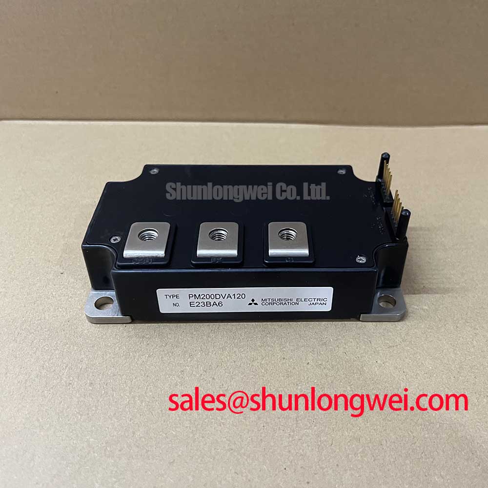
Begin a replacement assessment by checking the nameplate, inspecting the module body and terminals, and confirming that the original circuit was built around a 1200 V, 200 A Mitsubishi Electric IPM. The supplied official product data identifies PM200DV1A120 as a Mitsubishi IPM Module with a rated voltage of 1200.0 V and a rated current of 200.0 A. These values define the component identity, but they do not by themselves establish the allowable current under every switching frequency, case temperature, cooling condition, or overload profile.
Before energizing a repaired industrial inverter welder or medium frequency induction heating power supply, compare the original wiring, gate drive architecture, protection signals, cooling arrangement, and DC link topology with the replacement installation. The system integrator should verify the complete Mitsubishi Electric documentation for terminal assignment, electrical isolation, switching conditions, protection timing, and thermal limits before applying operating voltage. The public Mitsubishi Electric Power Semiconductors and High Power Modules resource is an appropriate manufacturer reference point for power device documentation.
| Item | Specified information | Engineering use |
|---|---|---|
| Manufacturer | Mitsubishi Electric | Confirm the control and power circuit documentation against the original equipment |
| Part number | PM200DV1A120 | Use the complete marking when checking replacement compatibility |
| Device category | IPM Module | Evaluate the module as part of its complete gate drive and protection system |
| Rated voltage | 1200.0 V | Compare with measured DC link voltage and switching transients |
| Rated current | 200.0 A | Compare with load current, duty cycle, temperature, and cooling conditions |
The 1200 V and 200 A figures are Official Specification values supplied for this product page. They are not a substitute for the complete data sheet curves. A repair engineer should record the DC link voltage during startup, standby, load operation, and regenerative events. Oscilloscope measurements should use a suitable differential probe and a controlled test procedure. A current rating comparison also requires attention to pulse duration, switching loss, junction temperature, heat sink performance, and the actual waveform rather than only an RMS meter reading.
For a circuit that also contains a controlled rectifier stage, the CM100DY 12E may be reviewed as a neutral reference for the upstream rectification section. It should not be treated as an automatic companion or replacement for any part of the original topology. The rectifier control angle, line impedance, firing circuit, DC link capacitance, and braking path all influence the electrical stress eventually seen by the IPM.
Benchtop Waveform Tuning: Managing Capacitive Gate Coupling
Connect the oscilloscope at the actual gate drive reference and compare the commanded gate waveform with the voltage measured at the module terminal. During a high voltage switching event, the displacement current associated with device capacitance can couple through the gate loop and create an unintended gate voltage excursion. This is a Design Consideration, not a confirmed internal parameter of PM200DV1A120. The resulting waveform should be assessed for false turn on, excessive ringing, delayed turn off, and abnormal overlap between the upper and lower switching paths.
A low impedance gate loop is normally preferred because long conductors add inductance and allow the gate voltage to move with the power switching node. Keep the drive return physically close to the corresponding gate connection, separate the high current commutation path from the control return, and avoid routing sensitive protection signals alongside the collector or switching node. The final arrangement is system determined because the correct gate resistance, driver current, dead time, clamp strategy, and isolation method depend on the module circuit and switching frequency.
An active Miller clamp can be considered where the driver architecture supports it. Its purpose is to hold the gate at a defined low state during the opposite switch transition, reducing the chance that capacitive coupling produces an unintended command. A negative gate bias is also an application option in some drive systems, but the allowable value for this module must be verified from the original Mitsubishi Electric drive requirements. Do not assume that a negative bias range shown in a general application note is automatically suitable for this specific module.
For bench troubleshooting, first capture the gate to emitter waveform under a low energy test condition. Then compare it with the collector to emitter switching waveform and the driver fault output. If the gate waveform changes substantially when the power loop is connected, review common impedance, probe grounding, auxiliary terminal routing, and isolation capacitance. If the gate remains stable but the collector waveform overshoots, the primary investigation should move to commutation inductance and clamping rather than immediately changing the gate resistor.
Dead time should be verified against the measured turn off and turn on behavior of the complete system. A longer command dead time can reduce overlap risk, but it can also increase conduction loss and alter the output waveform. The appropriate value is therefore a system validation result rather than a universal PM200DV1A120 setting. Protection desaturation, overcurrent feedback, undervoltage lockout, and fault reset behavior should be checked independently before high energy testing.
Pro Tip: Keep the gate drive return separate from the high current emitter path until the module terminal arrangement has been verified from the correct Mitsubishi Electric documentation.
When comparing a different high power module for mechanical or electrical evaluation, engineers may also review SKIIP37AC12T4V1 as a separate reference. Similar voltage or current descriptions do not prove pin compatibility, drive compatibility, thermal equivalence, or protection compatibility.
Operational Boundary Review for Altitude and Regenerative Bus Events
High altitude operation should be treated as a system qualification subject rather than assigned a universal failure rate for this module. Reduced air density can affect cooling and external insulation coordination, while terrestrial radiation exposure can be relevant to high voltage semiconductor reliability. No FIT value, Single Event Burnout limit, cosmic ray failure probability, or altitude derating curve is provided in the supplied product information. Those figures should not be invented or presented as PM200DV1A120 field data.
For an installation above the equipment maker’s normal environmental range, measure the actual heat sink temperature, case temperature, air movement, enclosure pressure condition, and DC link voltage under the intended load. Review the manufacturer’s environmental qualification documents and the applicable equipment safety standard. The Mitsubishi Electric Global Semiconductor Device Technologies resource can help locate manufacturer level technical information, but the system designer remains responsible for confirming the applicable rating and derating conditions.
Thermal interface material selection and application are Design Considerations. The interface should be continuous, clean, and compatible with the module base and heat sink surface. Excess material can increase thermal resistance, while inadequate coverage can leave air gaps. Mounting pressure should be applied progressively and evenly according to the manufacturer’s mechanical instructions. A cross pattern may help distribute pressure on a multi fastener assembly, but the correct screw type, torque, washer arrangement, and sequence must come from the applicable mechanical documentation rather than a generic rule.
Regenerative operation requires a separate energy review. During motor deceleration, energy can raise the DC link voltage if the active front end, braking transistor, braking resistor, or control system cannot absorb it at the required rate. The PM200DV1A120 voltage rating should be compared with the measured peak DC link waveform, including switching overshoot and control fault conditions. The braking path must be evaluated for pulse energy, repetition rate, resistor thermal capacity, semiconductor conduction loss, and protective shutdown behavior.
A practical test begins with a controlled deceleration at reduced stored energy. Record the DC link voltage, braking command, resistor current, module temperature, and fault timing. Repeat the measurement across the intended speed and load range only after the first waveform is understood. If the DC link rises unexpectedly, inspect the brake command signal, resistor continuity, contactor state, current sensor polarity, and controller thresholds as a group. One symptom should not be assigned to one component without comparing the complete signal path.
For industrial inverter welders, the transformer or output inductor can return energy to the DC link during a rapid current change. For medium frequency induction heating equipment, resonant behavior can produce voltage movement that is strongly dependent on the work coil, matching network, switching frequency, and load condition. The engineering discussion in Resonant Topologies in Home Appliances provides useful topology context, while the PM200DV1A120 installation still requires direct measurement of the actual equipment waveform.
High Frequency Commutation Loop and Transient Verification
Inspect the physical DC link and switching loop before changing semiconductor settings. The positive rail, module terminals, return rail, snubber path, and capacitor connection should form the smallest practical commutation loop allowed by the equipment insulation and mechanical structure. This is an Engineering Recommendation intended to reduce parasitic inductance and turn off voltage overshoot. The suitable geometry must be validated with a properly connected oscilloscope because probe placement can introduce an apparent spike that is not present at the device terminals.
The transient relationship can be considered in the usual engineering form: the peak switching voltage rises with the DC link voltage and with the product of commutation inductance and current change rate. This is an Engineering Calculation principle, not an official PM200DV1A120 limit. The designer should compare the measured peak with the voltage boundary, temperature condition, switching command, and protection response specified for the complete system. A target such as a particular nanohenry value should not be assigned without the mechanical stack up, current waveform, busbar geometry, and validated measurement method.
Snubber selection should follow the measured ringing frequency, energy, pulse repetition, and capacitor voltage stress. A capacitor value copied from another inverter may produce excessive circulating current or insufficient damping in this circuit. Place the snubber path close to the switching terminals when the mechanical and insulation design permits it, and keep its return path short. The final capacitor, resistor, and mounting arrangement are system determined and should be verified by thermal measurement as well as waveform capture.
During troubleshooting, compare the voltage at the module terminals with the voltage measured across the nearby DC link capacitor. A large difference can indicate layout inductance, an ineffective snubber connection, a damaged capacitor, or a measurement loop problem. Check the waveform at several load currents and switching commands. If the ringing frequency remains similar while the amplitude changes with current, the commutation network deserves close review; this observation alone does not identify a failed module.
Symmetrical planar busbar geometry can reduce unequal current sharing between parallel paths and can make the switching waveform easier to control. It must still provide adequate creepage, clearance, mechanical support, and insulation for the 1200 V class circuit. Control wiring, fault feedback, and any auxiliary emitter or source reference should be routed according to the verified terminal definition. Do not assume that a terminal that appears electrically convenient is a Kelvin reference or an independent low inductance return unless the manufacturer documentation confirms it.
Complete the final validation with controlled switching tests, thermal observation, fault interruption checks, and regenerative event testing. The acceptance decision should be based on measured voltage and current margins under the intended operating conditions, not solely on the printed 1200 V and 200 A identity values. This approach keeps the PM200DV1A120 evaluation tied to its official product data while leaving system level switching, cooling, protection, and mechanical decisions to documented engineering verification.