 IGBT/power device
The IGBT module is a modular semiconductor product that is packaged by IGBT (Insulated Gate Bipolar Transistor Chip) and FWD (Freewheeling Diode Chip) through a specific circuit bridge; the packaged IGBT module is directly applied to the inverter and the UPS is uninterrupted. Power supply and other equipment; IGBT module has the characteristics of energy saving, convenient installation and maintenance, and stable heat dissipation.
Installation of IGBT modules:
In order to make the contact thermal resistance small, it is recommended to apply a heat-dissipating insulating mixture between the heat sink and the mounting surface of the IGBT(MIG75Q202H) module. When the heat-dissipating insulating mixture is applied, it is applied to the surface of the metal substrate of the heat sink or IGBT module. As shown in Figure 1. As the IGBT module and the heat sink are clamped by screws, the heat-dissipating insulating mixture is dispersed, so that the IGBT module and the heat sink are in uniform contact.
Applying the same thickness of thermal paste (especially when the coating thickness is thick) can make the module without copper substrate more serious than the module with heat dissipation from the copper substrate, and finally the junction temperature of the module is beyond the safe operation of the module. The upper limit of the junction temperature (Tj "125 ° C or 125 ° C). The increase in the thickness of the thermal paste caused by the uneven surface of the heat sink increases the contact thermal resistance, thereby slowing the diffusion rate of heat.
When the IGBT module is installed, the clamping method of the screw is shown in Figure 2. In addition, the screws should be clamped to the recommended range of clamping torques. If the torque is insufficient, the contact thermal resistance may become large or loose during operation. Conversely, if the torque is too large, it may cause damage to the casing. When the IGBT module is mounted on a heat sink made of an extrusion die, the mounting of the IGBT module is parallel to the direction in which the heat sink is extruded, in order to reduce the influence of the deformation of the heat sink.
When soldering the module to the PCB, care should be taken that the soldering time is short. Pay attention to the amount of solvent desiccant used in the wave soldering machine. Do not use excessive solvent. The module cannot be flushed. The 50 μm heat-dissipating composite screw was printed on the surface of the heat sink by screen printing technology to mount the module and the PCB on the heat sink. A slight movement of the module allows for better distribution of the thermal grease before the screws are applied. When installing the screws, first fix the two screws with the appropriate force and then tighten the screws with the recommended force.
When the gate drive circuit and the control circuit are soldered at the terminals of the IGBT module, if the solder temperature is too high, problems such as melting of the case resin material may occur. Terminal heat resistance test conditions for general products: solder temperature: 260 ± 5 °C. Welding time: 10 ± 1 s. Number of times: 1 time.
Matters needing attention in the installation of IGBT modules:
1) To install without power supply, use anti-static measures such as grounding table, grounding ground and grounding wrist strap for loading and unloading. First, the static electricity on the body and clothes is discharged through a high-resistance (about 1Ωn) ground wire, and then operated on a grounded conductive pad. To take the package body, do not touch the terminal (especially the control terminal) directly. Do not subject the terminals of the module electrodes to excessive stress.
2) The heat sink of the IGBT module should be matched according to the use conditions and environment and the parameters of the IGBT module to ensure the requirements of the heat sink when the GBT module works. In order to reduce the contact thermal resistance, it is recommended to apply a thin layer of thermal grease between the heat sink and the IGBT module.
3) When the IGBT module is mounted on the heat sink, first apply the heat-dissipating insulation mixture (thermal grease) on the reverse side of the module, and then fully tighten it with the recommended clamping force. In addition, the flatness between the positions where the screws are mounted on the heat sink should be controlled below 100 μm, and the surface roughness should be controlled below 10 μm. If the surface of the heat sink is recessed, the contact resistance (Rth(c-f) increases. In addition, when the flatness of the surface of the heat sink is outside the above range, the IGBT module is installed (when clamped) to the inside of the IGBT module. The chip and the insulating substrate located between the metal substrates increase stress and may cause dielectric breakdown.
4) The IGBT module backplane is a copper plate module. After the heat sink and IGBT module are evenly stressed, it can be seen from the edge of the IGBT module that there is a little thermal grease extrusion. The bottom plate of the IGBT module is a module of the DBC substrate, and the surface of the heat sink must be flat and smooth. After coating a thin layer of thermal grease by screen printing or rolling, the two are uniformly crimped.
When the IGBT module is directly fixed on the heat sink, each screw should be tightened according to the torque given in the manual. The screw must be evenly stressed. If the torque is insufficient, the thermal resistance will increase or the screw will loose during the movement. When the fastening screws are installed at two points, the first and second ones are tightened to 1/3 of the rated torque in turn, and then repeatedly made to reach the rated torque. The four-point installation is similar to the two-point installation. When tightening the screws, tighten the 1/3 rated torque diagonally and then repeatedly to reach the rated torque.
5) The surface of the radiator should be smooth and clean. The flatness should be ≤150μm and the surface finish should be ≤6μm. The heat transfer conductive paste should be applied at the interface. The coating should be uniform and the thickness should be about 150μm.
6) When using a heat sink with a grain, the long direction of the IGBT module follows the grain of the heat sink to reduce the deformation of the heat sink. When two modules are installed on a radiator, they are placed side by side in a short direction, leaving a sufficient distance in the middle, which is mainly to reduce the heat superposition when the fan is dissipated, easy to dissipate heat, and maximize the efficiency of the radiator.
Internal wiring diagram of GA series IGBT single switch module

Igbt module physical wiring diagram analysis
IGBT drive circuit
The following figure shows the internal structure of the M57962L driver. The optocoupler is used for electrical isolation. The optocoupler is fast. It is suitable for high-frequency switching operation. The primary side of the optocoupler has series current limiting resistor (about 185 Ω), which can be 5 V. The voltage is applied directly to the input side. It uses a dual power supply structure, integrated with 2 500 V high isolation voltage optocoupler and overcurrent protection circuit, overcurrent protection output signal terminal and TTL level compatible input interface, drive electrical signal delay up to 1.5 Us.
When the M57962L is used alone to drive the IGBT. There are three points that should be considered. First of all. The maximum current rate of change of the driver should be set within the limits of the minimum RG resistance, because for many IGBTs, when RG is used too large, td(on) (on-delay time) is increased, td(off) (cut-off delay time), tr (rise time) and switching loss, this loss should be avoided as much as possible in high frequency applications (over 5 kHz). Also. The loss of the drive itself must also be considered.
If the loss of the drive itself is too large, it will cause the drive to overheat and cause damage. Finally, when the M57962L is used to drive large-capacity IGBTs, its slow turn-off will increase losses. The cause of this phenomenon is that the current flowing to the gate of the M57962L through the Gres (reverse transfer capacitor) of the IGBT cannot be absorbed by the driver. Its impedance is not low enough, this slow turn-off time will become slower and requires a larger snubber capacitor to apply the driver circuit of the M57962L design as shown below.
Circuit Description: Power supply decoupling capacitors C2 ~ C7 use aluminum electrolytic capacitors, the capacity is 100 uF / 50 V, R1 resistance value is 1 kΩ, R2 resistance value is 1.5kΩ, R3 is 5.1 kΩ, power supply uses positive and negative l5 V power supply module Connected to the 4th and 6th pins of the M57962L respectively, the logic control signal IN is input to the driver M57962L via the l3 pin. The bidirectional voltage regulator Z1 is selected to be 9.1 V, Z2 is 18V, and Z3 is 30 V. The gate and emitter of the IGBT are prevented from breakdown and the drive circuit is damaged. The diode adopts the fast recovery FR107 tube.
IGBT module wiring considerations:
1) The gate should be insulated from any conductive area to avoid static electricity and breakdown. The IGBT will have a conductive foam at the G and E poles during packaging and short-circuit it. When assembling, do not touch the G pole directly with your finger until the G pole is permanently connected before removing the short wiring between the G and E poles.
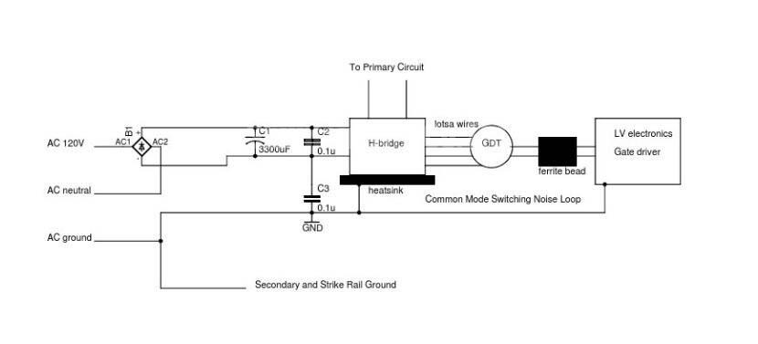
2) In the high-power inverter, not only the switching tubes of the upper arm should use independent isolation power, but also the independent switching power supply of the lower arm to avoid loop noise. To achieve a certain level of insulation requirements.
3) When connecting the IGBT electrode terminals, there should be no tension and pressure between the main terminal electrodes. The connecting wires (strips) must meet the application to prevent the electrode terminals from heating up and overheating on the module. The control signal line and the drive power line should be far apart, as vertical as possible, and not placed in parallel.
4) The trace on the PCB between the optocoupler output and the IGBT input should be as short as possible, preferably no more than 3cm.
5) Drive signal isolation High-speed optocoupler with high common mode rejection ratio (CMR) is required. tp "0.8μs, CMR" l0kV/μs, such as 6N137, TCP250, etc.
6) The black sleeve on the drive terminal of the IGBT module is an anti-static conductive tube. When using the connector lead, the lead should be inserted immediately after removing the sleeve; or when the soldering lead is used, the sleeve is first welded and then cut.
7) When soldering the IGBT terminal, in order to avoid static electricity from the soldering iron and soldering iron soldering station, the soldering iron front end should be grounded with a very low resistance. When soldering the G pole, the soldering iron should be powered off and grounded. It is most suitable to use a fixed temperature soldering iron. When soldered by hand, the temperature is 260 ° C ± 5 ° C, time (10 +1) s. When soldering the wave, the PCB should be preheated at 80 ~ 105 ° C, and immersed in solder for 3 ~ 4 s at 245 ° C.
8) When measuring the instrument, 1000 resistors should be used in series with the G pole. When measuring the drive voltage (VGE) at the terminal of the module, be sure to add a predetermined voltage.
9) The IGBT module is discharged in a state where antistatic measures are taken against the control terminals with a conductive material such as lC foam. This conductive material can be removed after the product is electrically connected.
10) When only FWD is used instead of IGBT (for example, when applied in a chopper circuit, etc.), a reverse bias of -5 V or more (recommended -15 V, maximum – 20 V) should be added between G-Es of unused IGBTs. When the reverse bias is insufficient, the IGBT(CM400HA-12H) may be damaged due to false triggering caused by dv/dt in the reverse recovery of the FWD.